8 layer PCB is suitable for complex electronic products that require high circuit density, such as computer motherboards, audio equipment, and network equipment, and is a popular choice in the electronics industry. Known for supporting fast signal transmission and providing greater flexibility in component placement, 8-layer PCBs play an integral role in advanced electronic systems. This article delves into the complexity of 8 layer PCBs, covering their functionality, design guidelines, and key prototyping processes.
An 8-layer PCB stackup refers to the arrangement of eight distinct layers within a printed circuit board. Each layer serves a specific purpose, contributing to the overall functionality and performance of the PCB. The stackup is a crucial aspect of PCB design, influencing factors such as signal integrity, power distribution, and thermal management. The typical composition of an 8-layer PCB stackup includes:
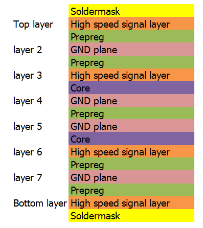
Top Signal Layer: The top layer is dedicated to routing signals, connecting various components on the PCB.
Ground Plane (Layer 2): The second layer is often a ground plane, providing a stable reference for signal return paths and aiding in electromagnetic interference (EMI) reduction.
Power Plane (Layer 3): This layer is dedicated to power distribution, supplying power to the components on the PCB.
Signal Layer (Layer 4): Another signal layer for additional routing flexibility.
Inner Ground Plane (Layer 5): Similar to the second layer, this ground plane further contributes to EMI reduction and signal integrity.
Inner Power Plane (Layer 6): Another layer for power distribution, ensuring a stable supply to components.
Signal Layer (Layer 7): Another signal layer, allowing for intricate routing of signals.
Bottom Signal Layer: The bottom layer serves as the counterpart to the top signal layer, completing the routing of signals.
The thickness of an 8 layer PCB stackup can vary based on several factors, including the choice of materials, copper thickness, and overall design specifications. Generally, the total thickness of an 8-layer PCB stackup falls within a range of 0.062 inches (1.57 mm) to 0.093 inches (2.36 mm). However, this is a broad estimate, and actual thickness can be customized to meet specific requirements.
The breakdown of the layers contributes to the overall thickness, and typical layer thicknesses include:
Copper Layers: The thickness of copper layers is usually specified in ounces per square foot (oz/ft²). Common choices are 1 oz/ft² (approximately 35 µm) or 2 oz/ft² (approximately 70 µm), but higher copper weights are also possible for specialized applications.
Prepreg Layers: Prepreg, or pre-impregnated fiberglass layers, are used to bond the core layers together. The thickness of prepreg layers can vary, with common choices being 0.002 inches (50 µm) or 0.003 inches (75 µm).
Core Layers: The core layers, which are typically made of fiberglass-reinforced epoxy resin, contribute to the overall thickness. The core thickness can vary based on the specific design requirements.
Considering all these factors, an 8-layer PCB stackup may have a core thickness of around 0.040 inches (1.02 mm) to 0.062 inches (1.57 mm), with the copper layers and prepreg layers adding to this total.
When embarking on the design of an 8-layer PCB, meticulous attention to key considerations ensures the reliability and optimal performance of the final product. One fundamental aspect is Impedance Control, where the designer must carefully measure and regulate trace impedance. Achieving this involves aligning substrate material properties with trace dimensions and locations, ensuring that signal trace impedance adheres to specified values for optimal board performance.
The necessity to shield signal layers from one another is driven by the aim to prevent signal loss and interference. Leveraging the inherent advantage of featuring multiple planes, an 8-layer PCB becomes an efficient shield for signal layers, contributing significantly to enhanced signal integrity—a pivotal reason for the prevalent preference for these designs.
The mitigation of noise is a crucial facet in 8-layer PCB design. Preventing Noise Decoupling demands proactive measures. Establishing a digital ground plane serves as a robust solution to this challenge. This ground plane facilitates the design of multiple ground and power planes, strategically deployed throughout the stackup, thus preemptively preventing potential noise-related issues.
Achieving a harmonious and structurally sound 8-layer stackup involves meticulous attention to Layers Balancing. This necessitates the creation of a balanced stackup with symmetrical cross-sectional structures and layer surfaces. By removing areas prone to deformation during manufacturing stresses, designers contribute to the overall structural robustness of the PCB. A thorough evaluation of the circuit layout by the PCB manufacturer becomes imperative in this regard.
Click here to see the perfect stackup for high-speed design
Multilayer PCBs offer advantages crucial in diverse electronic applications. The heightened density accommodates intricate circuits and components, making them apt for complex designs. With dedicated ground and power planes, multilayer PCBs enhance signal integrity by minimizing electromagnetic interference and crosstalk, ensuring reliable performance.
The compact nature of multilayer PCBs reduces overall size and weight, beneficial in space-constrained environments. Efficient power distribution and improved thermal performance further contribute to their appeal. Designers appreciate the flexibility to route traces across multiple layers, providing versatility without compromising external dimensions.
However, these advantages come with considerations. The increased cost of manufacturing multilayer PCBs stems from their complexity and additional materials. The intricate manufacturing process introduces challenges, potentially leading to defects. While signal integrity is generally enhanced, improper design or layer stacking can pose challenges.
Despite their complexity, multilayer PCBs remain an integral part of advanced electronics, offering reliability and functionality in diverse applications. Understanding both their merits and considerations is imperative for informed decision-making in electronic design.
Choosing between a 6-layer pcb and an 8-layer PCB involves considering specific requirements and trade-offs based on the complexity of the electronic design. Here’s a comparison of the two:
| Aspect | 6-Layer PCB | 8-Layer PCB |
|---|---|---|
| Cost | Generally more cost-effective | Generally more expensive |
| Design Complexity | Simpler design process | Supports highly complex designs |
| Component Density | Suitable for moderate complexity | Ideal for high component density and intricate routing |
| Signal Integrity | Fewer layers may pose some challenges | Enhanced signal integrity management |
| Power Distribution | Adequate for simpler power distribution | Allows for more efficient power distribution |
| Thermal Management | Limited options for thermal dissipation | Enhanced thermal dissipation options |
| Manufacturing Complexity | Less complex manufacturing process | More intricate manufacturing process |
| Suitability | Suitable for projects with budget constraints | Ideal for projects with higher complexity and budgets |
If the design is relatively simple, cost is a significant consideration, and signal integrity challenges are manageable with fewer layers, a 6-layer PCB may be a suitable choice.
For complex designs with higher component density, stringent signal integrity requirements, and the need for efficient power distribution and thermal management, an 8-layer PCB might be more appropriate.
8-layer PCBs find application in a variety of industries and electronic devices that demand a higher level of complexity and functionality. Here are some common applications:
Computer Motherboards: 8-layer PCBs are frequently used in computer motherboards where there is a need for a high component density, complex routing, and efficient power distribution.
Telecommunications Devices: Communication devices, such as mobile phones and base stations, benefit from the higher layer count to support the complex radio frequency (RF) designs and signal processing.
Automotive Electronics: Advanced automotive systems, such as engine control units (ECUs), navigation systems, and safety features, leverage 8-layer PCBs for their ability to handle intricate electronics.
Aerospace and Defense Electronics: In aerospace and defense applications, where reliability is critical, 8-layer PCBs are used in avionics, radar systems, and communication equipment.
Selecting the best 8-layer PCB manufacturer is a critical decision that directly impacts the performance and reliability of your electronic devices. Here are key considerations to guide you in choosing the most suitable manufacturer.
Choose an 8-layer PCB manufacturer with the right skills and experience. Ask how long they’ve been in the business and what certifications they have. This ensures they can handle the complexity of 8-layer stackups and meet your specific requirements.
Consider how quickly the manufacturer can finish making your circuit boards. Look for reviews from other clients to see if the manufacturer is known for working efficiently and meeting deadlines.
Check if the manufacturer can produce the quantity of boards you need. Some may only handle small orders, so if you need a lot of 8-layer PCBs, make sure they can handle larger quantities.
Good customer service means the manufacturer is always available to help and responds quickly. Choose a manufacturer that not only meets your demands but also provides helpful advice. This ensures a smooth and successful collaboration on your 8-layer PCB project.
Are you ready to elevate your electronic designs with top-notch 8-layer PCBs? Look no further! As a leading PCB manufacturer, VictoryPCB brings a wealth of expertise, advanced technology, and a commitment to quality to meet your project’s demands. Contact us today for a quote, expert consultation, or to discuss how our 8-layer PCB solutions can enhance your designs. Your success is our priority. Let’s build excellence together!
10 Layer PCB: Essential Guide for PCB Stackup Design & Applications


