High-Density Interconnector (HDI) PCBs are essential in modern electronics, offering advanced technology that makes electronic devices smaller, faster, and more efficient. Unlike traditional PCBs, HDI PCBs use finer lines and spaces, smaller vias, and capture pads, and higher connection pad density. This introduction will briefly explore what HDI PCBs are and why they are crucial in today’s electronic world.
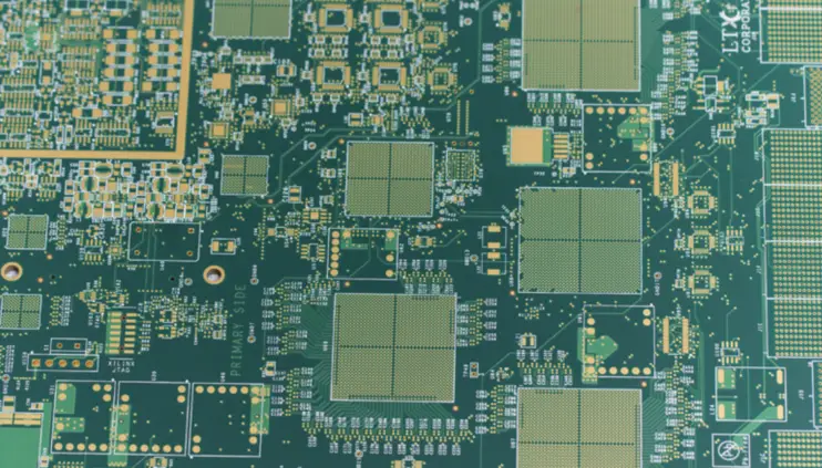
HDI PCB is a special kind of printed circuit board that pack more wiring into a smaller space compared to regular PCBs. HDI PCBs are known for certain features like microvias, blind and buried vias, and built-up laminations, all of which help in enhancing signal performance. The world of electronics is always changing, with a constant push for devices that are smaller and faster. HDI boards fit perfectly into this trend as they are more compact. They have tinier vias (which are like small tunnels in the PCB for passing connections), pads, copper traces, and spaces. This compactness leads to wiring that is more densely packed, making the boards lighter, smaller, and with fewer layers.
A data report recorded that HDI (high density interconnect) usage/fabrication has increased from 37.5% to just over 49% in five years, So HDI boards are growing quickly in popularity in the PCB industry. These boards often include very small vias that are 0.006 inches or less in diameter. Thanks to their high circuitry density, they can perform the functions of multiple traditional circuit boards all by themselves. This ability makes them a go-to choice for modern electronic devices that require advanced functionality packed into a limited space.
High-Density Interconnect PCBs offer numerous benefits that are crucial in the rapidly evolving electronics industry. These benefits stem from their advanced design and manufacturing techniques.
Miniaturization: One of the primary advantages of HDI PCBs is their ability to support miniaturization. As electronic devices become smaller and more powerful, HDI PCBs play a critical role in enabling this trend. They can pack more functionality into a smaller space due to their denser wiring and smaller components.
Enhanced Performance: HDI PCBs have improved electrical performance. They achieve this by shortening the path that electrical signals must travel. This reduction in signal paths leads to faster signal transmission and reduces the risk of signal loss or interference. Consequently, devices using HDI PCBs are not only compact but also faster and more reliable.
Reduced Weight and Volume: With the higher circuitry density, HDI PCBs require fewer layers and less material. This results in lighter and thinner boards, which is especially beneficial for portable and wearable devices. The reduced weight and volume contribute to the overall lightness and compactness of the final product.
Cost-Effective in Long Run: While the initial cost of manufacturing HDI PCBs may be higher due to their complexity, they can be more cost-effective in the long run. This efficiency arises from the integration of multiple functions onto a single board, reducing the number of separate PCBs required in a device.
Improved Reliability: The advanced manufacturing processes of HDI PCBs result in boards with higher reliability. The use of microvias and other HDI-specific features contributes to stronger physical connections within the board. This enhanced robustness makes HDI PCBs ideal for applications in demanding environments where durability is a necessity.
High-Density Interconnect PCBs, while offering significant advantages in terms of miniaturization and performance, also present some challenges and disadvantages:
Higher Cost: The production of HDI PCBs typically involves more advanced and intricate manufacturing processes, which can lead to higher costs. The use of microvias, blind and buried vias, and other complex structures requires precise and sophisticated technology, often resulting in increased production costs.
Complex Design and Manufacturing Process: HDI PCBs demand a higher level of design precision and manufacturing expertise. The complexity of designing these boards, with their small size and dense circuitry, requires specialized skills and more advanced software tools. This complexity can extend the design phase and require more rigorous testing and validation, which can impact time-to-market.
Repair and Rework Challenges: Due to their small and densely packed components, HDI PCBs can be more challenging to repair or rework if issues arise. The compact nature of these boards makes it difficult to isolate and fix specific components without affecting neighboring parts, leading to potential increases in repair costs and time.
Limited Availability of Materials and Components: Some of the materials and components used in HDI PCBs may not be as readily available as those used in traditional PCBs. This limitation can affect production lead times and the overall availability of HDI PCBs.
HDI PCBs with the designations (1+N+1) and (2+N+2) refer to specific configurations of their layer structures. These configurations are part of what makes HDI technology so adaptable and efficient for creating compact, high-performance printed circuit boards.
This structure denotes an HDI PCB with a build-up of one layer on each side of a core.
The “1” represents one layer of microvias (small, high-density vias) on the top and one on the bottom of the PCB.
The “N” refers to the number of standard PCB layers in the core.
This structure allows for a simpler HDI design, providing a good balance between increased circuit density and manufacturability. It’s a step up from traditional PCB designs, offering better miniaturization and performance without being as complex or expensive as higher-order HDI structures.
This configuration indicates a more complex HDI PCB, with two layers of microvias on both the top and bottom sides of the core.
The “2” at each end signifies two layers of high-density microvias, which can be stacked or staggered, allowing for even greater density of connections.
As with the 1+N+1 structure, “N” represents the number of traditional PCB layers in the core.
The 2+N+2 structure is more advanced and allows for even greater miniaturization and more complex circuits. It is typically used in highly sophisticated electronic devices where space is at a premium, and a high number of connections is required.
Both these HDI structures enable the production of smaller, more efficient PCBs with a higher count of interconnections than traditional PCBs. The choice between (1+N+1) and (2+N+2) depends on the specific requirements of the electronic device, such as the complexity of the circuit, space constraints, and performance requirements.
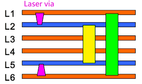
Firstly, through vias from surface to surface, combined with buried vias and through vias, represent a common configuration. This design allows for connections from one side of the board to the other, as well as concealed vias within the inner layers, optimizing space utilization.
Another type involves the integration of two or more HDI layers with through vias. This approach enhances routing density, permitting intricate and dense circuitry, crucial for modern electronic devices.
Some HDI PCBs incorporate passive substrates with no electrical connection. These non-functional layers provide mechanical support and insulation, contributing to the overall structural integrity of the board.
Coreless construction using layer pairs is an innovative design where traditional cores are omitted, and adjacent layers work as pairs. This method reduces weight and improves flexibility without compromising performance.
Additionally, alternate constructions of coreless designs using layer pairs offer adaptability in meeting specific project requirements. This flexibility allows for tailoring the HDI PCB to different applications, ensuring optimal performance in diverse technological landscapes.
When working with fine-pitch Ball Grid Array (BGA) components in High-Density Interconnect (HDI) layouts, certain essential guidelines apply to ensure a smooth design and fabrication process.

Check Manufacturer’s Capabilities: Always verify your manufacturer’s capabilities before embarking on an HDI design. Not all manufacturers offer the same capabilities, so it’s crucial to confirm compatibility to avoid issues during fabrication.
Mind Traces and Pads Spacing: Pay close attention to the spacing between traces and pads, especially in 1 mm pitch BGAs. Adjust solder mask clearance in line with your trace width, considering pad size and pitch to maintain a consistent design.
Avoid Unnecessary Staggered Vias and ELIC: Resist the temptation to use staggered vias or Extra-Large Inner Connects (ELIC) unless absolutely necessary. HDI routing aims to maximize surface and inner layer space, so only use additional features when they significantly contribute to your design.
Optimize Layer Count: Opt for fewer layers whenever possible. High layer counts increase manufacturing complexity and costs. By adhering to spacing guidelines, you can effectively reduce the overall cost per board.
Prioritize Signal Integrity: Don’t overlook signal integrity in HDI board designs. Whether dealing with high-speed or RF boards, apply the same signal integrity principles, adjusting for scale. Impedance-controlled routing is crucial, demanding careful consideration of trace design and stackup to maintain consistency with signaling standards.
The High-Density Interconnect PCB manufacturing process is specialized and distinct from traditional PCB manufacturing, emphasizing miniaturization and increased complexity. The key steps include design, material selection, laser drilling for microvias, layer lamination with insulating materials, copper plating and etching for precise circuit patterns, application of advanced surface finishes like ENIG, precise solder mask application, and component assembly using automated techniques. The process prioritizes the use of microvias, fine-pitch components, and multiple closely stacked layers. Rigorous testing and quality control ensure the reliability of the intricate circuitry, making HDI PCBs suitable for modern electronic devices requiring smaller form factors and enhanced functionality.
HDI PCBs find applications in various industries due to their compact design, increased functionality, and improved performance. Some notable applications of HDI PCBs include:
HDI PCBs are extensively used in smartphones, tablets, and other mobile devices where space is limited. The miniaturization achieved through HDI technology allows for the integration of complex circuitry in small form factors.
In computers and laptops, HDI PCBs contribute to the development of compact and high-performance systems. They are particularly beneficial in applications where there is a need for densely packed components and high-speed data processing.
HDI PCBs play a crucial role in medical electronics, where space constraints and reliability are paramount. They are used in devices such as medical imaging equipment, diagnostic tools, and wearable health monitoring devices.
The automotive industry relies on HDI PCBs for various applications, including advanced driver assistance systems (ADAS), in-vehicle infotainment (IVI) systems, and engine control units. The compact design and improved signal integrity are essential in automotive electronics.
HDI PCBs are employed in aerospace and defense applications for their reliability and ability to withstand harsh environmental conditions. They are used in communication systems, radar systems, navigation equipment, and other critical components.
HDI PCBs play a key role in telecommunications infrastructure, including base stations, transceivers, and networking hardware. The high-density interconnects enable efficient signal transmission and reception.
The evolution of High-Density Interconnect PCB technology promises to bring forth several impactful trends and developments. One significant trajectory involves the ongoing refinement of miniaturization techniques. The relentless pursuit of smaller form factors and increased component density is driven by the ever-growing demand for compact, high-performance electronic devices.
Another noteworthy trend is the integration of artificial intelligence (AI) and machine learning (ML) into HDI PCB design. This means smarter and more efficient layouts, enhancing the capabilities of electronic systems. Additionally, there’s a move towards using advanced materials that support high-speed data transmission, crucial for technologies like 5G communication.
When choosing a HDI PCB manufacturer, several critical factors should be considered to ensure the successful realization of your electronic designs. Here are key considerations:
Technical Expertise: Evaluate the manufacturer’s technical capabilities, especially in HDI technology. Ensure they have the expertise in laser drilling, microvias, and other advanced techniques necessary for intricate HDI PCB designs.
Quality Standards: Assess the manufacturer’s commitment to quality. Look for certifications such as ISO and UL, and inquire about their quality control processes to ensure that the produced PCBs meet industry standards.
Customization and Flexibility: Check if the manufacturer offers customization options to meet the specific requirements of your project. A flexible approach to design and production is crucial for adapting to diverse applications.
Lead Times and Production Capacity: Understand the manufacturer’s lead times and production capacity. Timely delivery is essential, and the ability to handle varying production volumes is advantageous for scalability.
VictoryPCB, a leading professional PCB manufacturer based in China. VictoryPCB specializes in the production of high-quality HDI PCBs, combining cutting-edge technology with a commitment to excellence. With years of experience in the industry, VictoryPCB has established itself as a reliable partner for those seeking advanced PCB solutions.
VictoryPCB boasts a team of skilled professionals with expertise in HDI technology, ensuring that intricate designs are executed with precision. The company adheres to stringent quality standards, holding certifications such as ISO 9001 and UL, guaranteeing the reliability and performance of their products.
Feel free to connect with VictoryPCB ([email protected]) to discuss your HDI PCB requirements, explore customization options, and experience the excellence that comes with our advanced technology and reliable service.


