The trace width, the measurement of a conducting copper pathway on a PCB, holds immense significance in ensuring efficient current flow, minimizing voltage drop, managing heat dissipation, and preserving signal integrity. In this article, we’ll discuss what is pcb trace and why is it important to consider when designing PCBs.
Trace width refers to the width or thickness of the conducting copper trace on a printed circuit board. It is an essential parameter that determines the current-carrying capacity and resistance of the trace. The width of the trace affects its ability to carry electrical current without excessive voltage drop or overheating.
The trace width is typically specified in terms of its dimensions, usually measured in millimeters (mm) or mils (1 mil = 0.001 inch). The trace width is important because it directly impacts the trace’s resistance and ability to handle the required current without causing excessive heat buildup.
Several factors are essential to consider when determining the appropriate trace width in PCB design.
The trace width should be sufficient to handle the expected current without causing excessive voltage drop or heating. Higher currents generally require wider trace widths to minimize resistance and prevent overheating.
The trace width affects the amount of heat generated during current flow. A wider trace can dissipate heat more effectively than a narrower trace. Consider the acceptable temperature rise for your application and select a trace width that can handle the required current while staying within the temperature limits.
Here is a chart that shows several trace widths and corresponding current values that will limit your temperature rise to 10 °C with 1 oz/square feet copper weight. This chart should give you an idea of the most suitable trace width in your PCB design.
| Current/A | Track Width(mil) | Track Width(mm) |
| 1 | 10 | 0.25 |
| 2 | 30 | 0.76 |
| 3 | 50 | 1.27 |
| 4 | 80 | 2.03 |
| 5 | 110 | 2.79 |
| 6 | 150 | 3.81 |
| 7 | 180 | 4.57 |
| 8 | 220 | 5.59 |
| 9 | 260 | 6.60 |
| 10 | 300 | 7.62 |
Note: IPC recommended track width for 1 oz cooper PCB and 10 degree temperature rise.
The thickness of the copper layer on the PCB, commonly measured in ounces (oz), impacts the current-carrying capacity of the trace. Thicker copper layers can handle higher currents, allowing for narrower trace widths. Be aware of the specific copper weight used in your PCB design.
In high-speed digital or analog circuits, trace width can impact signal integrity by affecting impedance. Controlled impedance traces may require specific widths to maintain signal quality and prevent signal degradation.
Copper has a positive temperature coefficient of resistance, meaning its resistance increases as temperature rises. This effect should be considered when selecting the trace width to ensure that the resistance increase due to heating is within acceptable limits.
Consider the manufacturing capabilities of your PCB manufacturer. They may have limitations on minimum trace width that can be reliably achieved during the fabrication process. Ensure that the chosen trace width aligns with the manufacturer’s capabilities.
The available space on the PCB may restrict the maximum trace width you can use. It is essential to strike a balance between the required trace width for current handling and the available space on the board.
PCB trace width, measured in mils or thousands of inches, is an important parameter in PCB design. Common signals have trace widths ranging from 7 to 12 mils and lengths up to several inches.
Generally, PCB trace thickness ranges from 0.008 Inch to 0.240 Inch and it must be consistent throughout the PCB. There are a wide variety of PCB boards on the market, including single panel, double panel and multilayer board. The thickness of the track also varies according to the structure and type of the circuit board.
No matter pcb trace width or pcb trace thickness, VictoryPCB can be adapted and adjusted according to PCB design requirements and application current overload capacity.
Here’s a table showing the width and thickness ranges for PCB traces.
| Trace Application | Width Range (mm) | Width Range (mils) | Thickness Range (oz) | Thickness Range (inches) |
|---|---|---|---|---|
| Low-current signals | 0.1 – 0.2 mm | 4 – 8 mils | 0.5 – 2 oz | 0.0007 – 0.0028 inches |
| Moderate current signals | 0.2 – 0.3 mm | 8 – 12 mils | 0.5 – 2 oz | 0.0007 – 0.0028 inches |
| Power traces | 0.3 – 1.0 mm or wider | 12 – 40 mils or wider | 1 – 3 oz or higher | 0.0014 – 0.0042 inches or higher |
To calculate the resistance of a PCB trace, you can use the following formula:
R = (ρ * L) / (W * T)
Where:
R is the resistance of the trace in ohms (Ω).
ρ (rho) is the resistivity of the trace material in ohm-meters (Ω·m).
L is the length of the trace in meters (m).
W is the width of the trace in meters (m).
T is the thickness of the trace in meters (m).
It’s important to note that this formula assumes the trace has a uniform width and thickness along its entire length. Additionally, it assumes that the trace material has a constant resistivity value, which may vary with temperature.
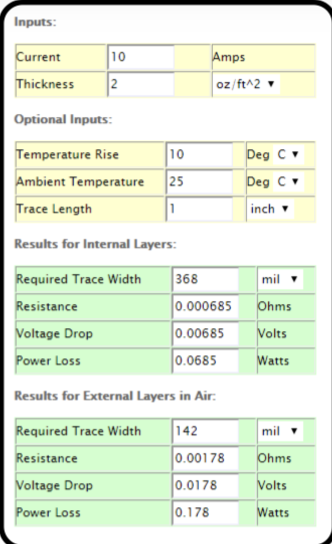
It is more convenient to use an online tool to calculate PCB trace resistance, such as the PCB Trace Width Calculator from CircuitCalculator, which can guide the choice of trace width when considering amperage.
Remember, apart from trace width, the shape of the trace and its location on the PCB can also impact signal reflection and noise immunity. For the best results, consider the overall design and consult with experts or specialized manufacturers to ensure the trace width aligns with your specific requirements.
By understanding the importance of trace width and considering various factors in the design process, you can optimize your PCB for efficient current flow, reduced voltage drop, effective heat dissipation, and reliable signal integrity.
To learn more about PCB design best practices and explore how trace width impacts your design, contact us at VictoryPCB and let our experienced team assist you in achieving high-quality, high-precision, and high-density PCBs for your applications.


