This article delves into the intricacies of the 6-layer PCB, shedding light on its design, the inherent advantages, and the best practices that have positioned it as a top choice for industry professionals. Whether you’re a seasoned designer or a curious enthusiast, this comprehensive guide will provide you with valuable insights into the world of 6-layer PCB stackups.
A 6-layer PCB refers to a Printed Circuit Board with six distinct layers. These layers are essential in modern electronics, enhancing both performance and reliability. Each layer has a specific function:
Signal Layers: These layers transmit data.
Power Layers: They distribute power to different parts of the board.
Ground Layers: These layers provide stability and prevent interference.
The use of a 6-layer PCB allows for more complex circuit designs, ensuring efficient communication between electronic components. As devices become more advanced, the demand for such PCBs increases. In business terms, opting for a 6-layer PCB means investing in durability, efficiency, and high performance.

The design above is a standard 6-layer PCB stackup. But it’s not suitable for every design. For example, high-speed designs typically always keep power and ground planes on adjacent layers for decoupling, while designs that require low electromagnetic emissions may need to utilize additional ground planes for shielding. A final practicality to consider is to always route vertically on adjacent routing layers. This helps improve routing efficiency and minimize crosstalk.
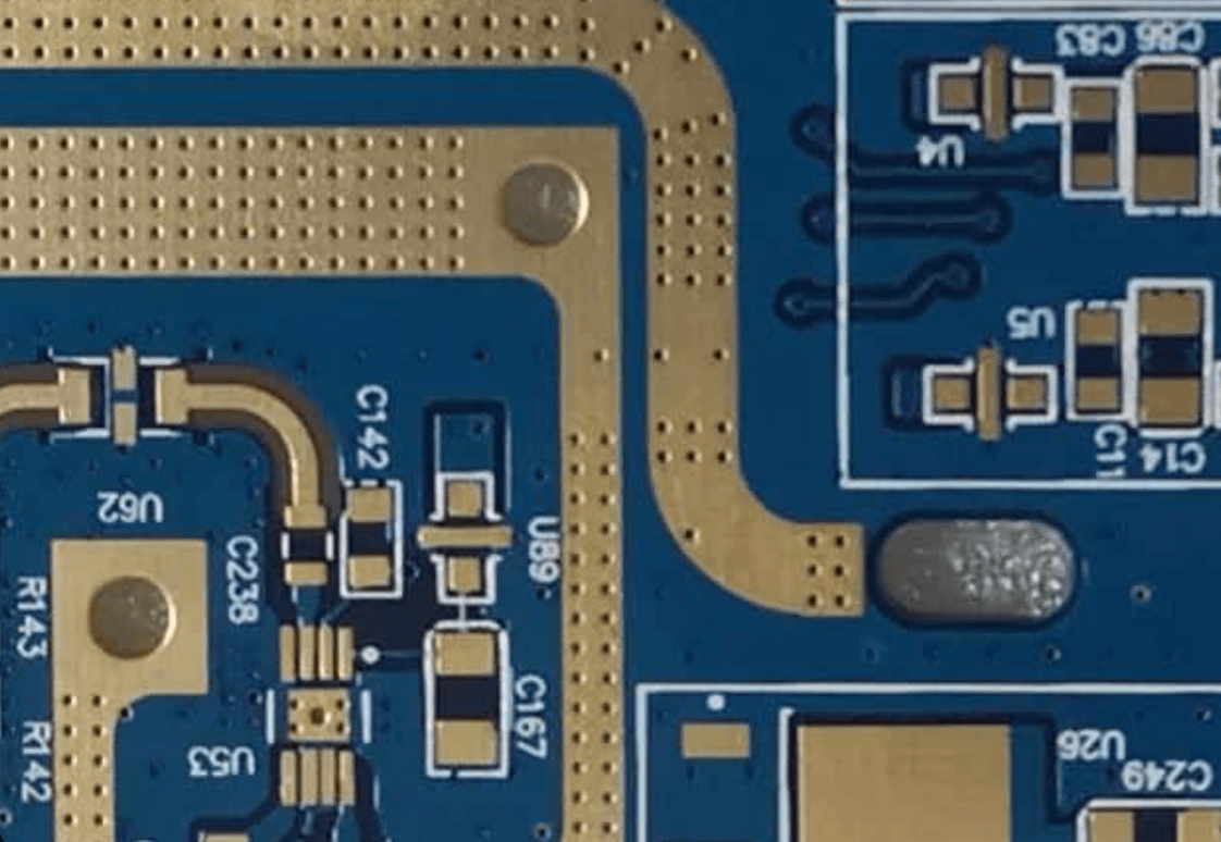
Here are some examples for other 6 Layer PCB Stackup:

While 4-layer PCBs have always been the first choice for many designers, the advent of 6-layer PCBs has changed the dynamic. There are several situations that make a 6-layer PCB a preferred choice over a 4-layer PCB:
If your 4-layer board uses SIG+PWR/GND/GND/SIG+PWR stackup and you are struggling with limited surface layer space for components, then a 6-layer PCB can be your savior. By relocating the PWR and SIG to the internal layers, not only do you gain more surface space, but you also achieve better decoupling via the PWR/GND plane pair.
For boards that handle both analog and digital signals, a 6-layer PCB offers the advantage of dedicating an entire surface layer to the analog interface. Additionally, it provides an additional internal layer tailored for slower digital routing to ensure minimal disruption.
If you are dealing with a high-speed board with a high input/output count, a 6-layer PCB provides an efficient layer separation strategy for signals, similar to the first point. This ensures a clearer signal path and reduces interference.
The decision to choose a 6-layer PCB isn’t just about adding layers; It is designed to enhance the overall functionality of the board, ensure optimal signal transmission and meet advanced requirements. As electronics continue to evolve, understanding and leveraging the benefits of 6-layer PCBs is critical for designers striving for efficiency and excellence.
Before diving into the routing process, it’s crucial to master the 6-layer PCB stackup. A stackup is an arrangement of six layers, usually including signal, power, and ground layers. Well-organized stacking ensures minimal interference, optimal signal integrity and efficient power distribution.
Signal layers: These layers are mainly used for routing signal traces. In a 6-layer PCB, you’ll often find signal layers on top, bottom, and sometimes even inside.
Power plane: Dedicated layers that distribute power to the board’s components. They provide a continuous path, ensuring stable power delivery.
Ground planes: These layers offer a return path for signals and help in reducing electromagnetic interference.
Maintain Impedance Control: Consistent impedance across traces ensures minimal signal reflection and loss. This is achieved by maintaining a uniform trace width and distance from the ground plane.
Avoid Crosstalk: Ensure that high-speed signal traces are adequately spaced apart to prevent interference. Using ground planes as shields between signal layers can also help.
Prioritize Critical Signals: Signals like clocks or sensitive analog signals should be routed first and kept as short as possible. They should also be kept away from noisy components or traces.
Use Vias Sparingly: While vias are essential for transitioning between layers, excessive use can introduce impedance discontinuities. It’s crucial to use them judiciously.
Power routing is the path that electricity takes on the PCB. Just like water flows through pipes to reach our homes, electricity flows through paths on the PCB to reach different parts. This electricity powers up the tiny parts on the board, making our devices work.
More Layers, More Power Needs: Since there are six layers, the PCB needs to make sure power reaches every layer correctly. It’s like ensuring every floor in a building gets water.
Avoiding Traffic Jams: Think of electricity as cars on a road. If all cars take the same route, there will be a traffic jam. Similarly, if too much electricity tries to go through one path, it can cause problems. A 6-layer PCB designs multiple routes for electricity to avoid such “traffic jams.”
Safety First: Just like we don’t want water to leak from pipes, we don’t want electricity to go where it shouldn’t. Proper power routing ensures electricity flows safely, without causing short circuits or damages.
Dedicated Power Layers: Some layers in the PCB are like main roads, designed only for electricity to flow. These are called power layers. They ensure that power reaches every part of the board efficiently.
Ground Layers for Stability: Ground layers act like the earth beneath our feet, providing stability. They make sure there’s no unwanted electricity floating around. This helps in preventing disturbances and keeps the device running smoothly.
Smart Design for Efficiency: Designers of the PCB plan the routes carefully. They make sure that power reaches faster to parts that need it the most. It’s like making sure hospitals get water supply first in a city.
EMC and EMI are crucial in electronics, especially in complex designs like 6-layer PCBs. For businesses, understanding and addressing these can lead to better products and happy customers. It’s all about ensuring that devices work as they should, without any unwanted “noise” or disturbances.
Proper Layering: In a 6-layer PCB, arranging the layers correctly can reduce EMI. It’s like placing barriers on roads to manage traffic better.
Ground Planes: These are like the “earth” of the PCB. They help in absorbing and reducing unwanted EMI, ensuring the device runs without hiccups.
Shielding: Some parts of the PCB might be more sensitive to EMI. Shielding is like putting a protective cover around these parts, so they remain unaffected.
Testing: Before a product reaches customers, it’s tested for EMC. It’s like checking a car’s brakes before selling it. This ensures that the device will work well in real-world conditions.
The 6-layer PCB, with its myriad advantages, is here to stay. As devices continue to shrink in size but grow in capabilities, the demand for compact, efficient, and high-performance PCBs will only rise. For anyone in the electronics domain, mastering the intricacies of the 6-layer PCB is not just beneficial – it’s essential.
Ready to experience the pinnacle of PCB design? As a leading PCB manufacturer in China, we specialize in crafting high-quality 6-layer PCBs tailored to your needs. Don’t compromise on performance or reliability. Choose the best for your projects. Contact us today and elevate your electronics with our expertly manufactured 6-layer PCBs!


