Professional PCB Manufacturer

China PCB Manufacturer

High-density Multilayer PCBs

What is HDI PCB

What is HDI PCB

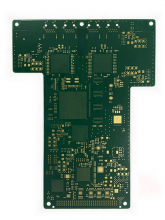
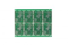
High Density Interconnect, or HDI, circuit boards are printed circuit boards with a higher wiring density per unit area than traditional printed circuit boards (PCB). In general, HDI PCBs are defined as PCBs with one or all of the following: microtraces, VIP (Via In Pad), microvias, blind vias, buried vias or other microvia technique, built-up laminations and high signal performance considerations.

Capabilities in Manufacturing HDI PCB

Victory PCB is a professional pcb manufacturer that can produce high-quality hdi PCB products. Check our PCB manufacturing capabilities in the following table:
Monthy Capability3900 m²/month
Layer10 Layers
MaterialFR4, TG180
Finished board thickness2m
Min Trace Width/Space3.5mil
Min hole size0.2mm
Min copper in hole thickness1oz
Outer layer Finished copper thickness1.5oz
Inner layer base copper thickness1oz
Impedance Control Tolerance±10%

Benefits and Challenges of Using HDI

  • Placement Feasibility – SMT Parts will not fit with room for pin escapes to PTH vias, so use VIP via in pad.

  • High Speed or RF performance – unwanted parasitics or excess inductance from standard PTH vias

  • Requirement for thin PCBs in some market spaces.

  • Back to back large active BGA’s on both sides of PCB.

  • RF on Primary Side / Digital on Secondary side

HDI uTraces - Using mSAP and SAP

Upcoming manufacturing process development will allow circuits to be designed with  lines and spaces in the range of 1-2 mil (25-50uM) with strict impedance control

mSAP – Modified Semi-Additive Process

With mSAP, a much thinner copper layer is coated onto the laminate, and plated in the areas where the resist is not applied thus, the “additive” nature of the process. The thin copper remaining in the spaces between conductors is then etched away. Whereas trace geometries are chemically defined during subtractive processes, mSAP allows trace geometries to be defined via photolithography.

SAP – Semi-Additive Process

Although the semi-additive process (SAP) used in the IC substrate board can realize more precise circuit fabrication, but there is a problem that the manufacturing cost is high and the production scale is small, thus restricted to ICs as of today

HDI PCB FAQs

  • 1. What is high density PCB?

    HDI PCBs have a higher circuitry density per unit than conventional PCBs. They use a combination of buried and blind vias, as well as microvias — those that are 0.006″ or less in diameter. High-density circuit boards are PCBs with one or more of the following features: Through vias and buried vias.

  • 2. What is the difference between HDI and standard PCB?

    HDI PCBs provide higher component density on smaller, lighter boards that generally have fewer layers to them when compared with traditional PCBs. HDI PCBs use laser drilling, micro vias, and have lower aspect ratios on the vias than with standard circuit boards.

  • 3. What are the advantages of HDI PCB?

    HDI boards are ideal where weight, space, reliability, and performance are primary concerns. Compact design: The combination of blind vias, buried vias, and microvias brings down the board space requirement.

  • 4. Where is HDI PCB used?

    Applications include mobile /cellular phones, touch-screen devices, laptop computers, digital cameras, 4/5G network communications, and military applications such as avionics and smart munitions.

Get custom hdi pcb that authenticates your business products and makes it an element for quick turnaround at a first go! At VictoryPCB, we work with each customer to ensure they get the boards they need, the way they need them. Contact us today for a quote for your specifications.


×

Contact Us

×

Inquire

*Name
*Email
Company Name
Tel
*Message

By continuing to use the site you agree to our privacy policy Terms and Conditions.

Recruit global agents and distributors Join us

I agree