A 4-layer PCB offers a versatile and efficient solution for various electronic applications. It consists of four layers of conductive material, typically copper, separated by insulating layers. This configuration allows for improved signal integrity, reduced noise interference, and increased routing density compared to single or double-layer PCBs.
In this article, we will delve into the world of 4-layer PCBs, exploring their design considerations, manufacturing process, and applications. We will examine the importance of selecting the appropriate thickness and stackup configuration, as well as provide guidelines for designing efficient and reliable 4-layer PCBs.
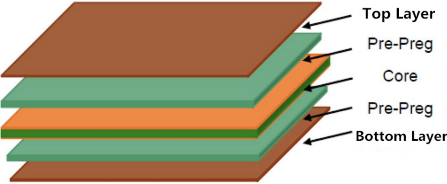
Generally, the layout of the 4-layer PCB consists of the top layer, the bottom layer, and two middle layers. The middle 2 layers are called the power layer, represented as VCC, and the ground layer represented as GND. The power layer and the ground layer can be isolated in the middle of the stackup to reduce interference.
The four-layer PCB comprises five different thicknesses, which are: 0.5mm, 0.8mm, 1.0mm, 1.2mm, and 1.6mm. This is pressed based on the double-sided PCB.
The thickness of a 4-layer PCB significantly impacts its mechanical strength, electrical performance, and overall functionality. Factors such as component height, mechanical stability, signal integrity, and impedance control must be carefully considered when determining the appropriate thickness for a specific application. Choosing the right PCB thickness ensures reliable operation, enhances performance, and contributes to the longevity of electronic systems.
Designing a 4-layer PCB requires careful attention to detail and adherence to specific guidelines to achieve optimal functionality, reliability, and manufacturability. Following the design guidelines such as proper layer stackup, signal and power plane separation, signal routing considerations, component placement, thermal management, DFM guidelines, and design validation, will help ensure efficient and high-performance PCB designs.
The layer stackup is a crucial aspect of 4-layer PCB design. It determines the arrangement and order of the copper and dielectric layers in the PCB. The stackup must be carefully planned to ensure proper signal integrity, controlled impedance, and ease of manufacturing. Considerations include placing power and ground planes appropriately, minimizing coupling and crosstalk, and optimizing the signal routing.
Separating the signal and power planes is essential for reducing electromagnetic interference (EMI) and maintaining signal integrity. Placing power and ground planes adjacent to each other helps to create a low-impedance return path for signals, minimizing noise and improving signal quality. Care should be taken to avoid routing high-speed signals over split power or ground planes, as this can introduce noise and signal degradation.
Proper signal routing is crucial for maintaining signal integrity and preventing signal distortions. Differential pairs, high-speed signals, and critical traces should be routed with controlled impedance, proper trace widths, and appropriate spacing. Signal length matching is also important to avoid timing issues and skew in high-speed designs. Utilizing design tools with length matching capabilities can help achieve precise length matching.
Efficient component placement plays a significant role in minimizing signal delays, reducing noise, and optimizing the routing process. Placing components strategically can shorten the trace lengths, reduce the number of vias, and improve signal integrity. Grouping related components together, such as decoupling capacitors near power pins, can enhance power distribution and reduce noise coupling.
Proper thermal management is essential for preventing excessive heat buildup, which can negatively impact component performance and reliability. In 4-layer PCB designs, ensuring adequate thermal vias and heat dissipation paths is crucial. Placing thermal vias under power components or near heat-generating components helps conduct heat away from critical areas, reducing the risk of overheating.
Designing a PCB with manufacturability in mind is vital to avoid potential fabrication and assembly issues. Following DFM guidelines such as maintaining minimum trace widths and clearances, adhering to solder mask and silkscreen requirements, and considering panelization requirements can help streamline the manufacturing process and minimize potential errors.
Before finalizing the design, it is essential to perform thorough design validation and testing. Using simulation tools, such as signal integrity analysis and thermal analysis, can help identify potential issues and ensure the design meets the desired specifications. Prototyping and testing the fabricated PCB also play a crucial role in verifying the design’s performance and functionality.
| Aspect | 2-Layer PCB | 4-Layer PCB |
|---|---|---|
| Number of Layers | 2 | 4 |
| Copper Thickness | Typically thicker copper layers | Thinner copper layers |
| Routing | Limited routing space | More routing space and flexibility |
| Complexity | Less complex | More complex, suitable for intricate designs |
| Signal Integrity | Moderate signal integrity | Improved signal integrity due to dedicated planes |
| Power Distribution | Limited power and ground planes | Dedicated power and ground planes |
| Thermal Dissipation | Less efficient heat dissipation | Better thermal management due to internal planes |
| Manufacturing Cost | Lower cost due to fewer layers | Slightly higher cost due to additional layers |
| PCB Size | Larger board size due to limited layers | Smaller board size with increased functionality |
| EMI and Crosstalk | More susceptible to EMI and crosstalk | Reduced EMI and crosstalk due to dedicated planes |
| Design Flexibility | Limited flexibility for complex designs | Increased flexibility for complex designs |
The cost of a 4-layer PCB can vary depending on several factors, including the complexity of the design, board size, quantity, material selection, and manufacturing processes. Generally, 4-layer PCBs tend to be slightly more expensive compared to 2-layer PCBs due to the additional layers and increased manufacturing complexity.
The 4-layer board is laminated based on the double-sided board. When lamination, PP, and copper foil are added on both sides of the double-sided board, it is then pressed into a multilayer board through high temperature and high pressure. In short, the 4-layer board has an inner layer. In terms of the process, some lines will be etched through the inner layer formed by lamination. The double-sided board can be drilled after cutting the raw material sheet directly.
Here are 4 layer pcb manufacturing process: Cutting material and grinding → drilling positioning holes → inner layer circuit → inner layer etching → inspection → black oxide → lamination → drilling → electroless copper → outer layer circuit → tin plating, etching tin removal → secondary drilling → inspection →print solder mask→Gold-plated→Hot air leveling→print silkscreen→routing outline→Test→Inspection.
4-layer PCBs find applications in various industries and electronic devices due to their increased functionality and design flexibility.Some common applications of 4-layer PCBs include: Communication Systems, Industrial Electronics — where they are often used in flow, pressure, level, and temperature measurement instruments — Medical Devices, Automotive Electronics, Consumer Electronics and Aerospace and Defense.
Are you seeking a trusted partner for 4 layer PCB manufacturing needs? Look no further! At VictoryPCB, we’re your go-to experts in producing top-tier multi-layer printed circuit boards.
Customization at Its Best: Whether you need a prototype or high-volume production, we tailor our services to your exact specifications. We pride ourselves on delivering customized solutions to meet your unique needs.
Quality Assurance: Quality is non-negotiable for us. Our stringent quality control measures ensure that every PCB leaving our facility meets the highest industry standards.
Timely Delivery: We understand the importance of deadlines. Count on us to deliver your multi-layer PCBs on time, every time.
Ready to elevate your PCB projects with precision and excellence? Contact us today to discuss your 4 layer PCB manufacturing requirements. Let’s turn your ideas into reality!


