The thickness of copper used in PCBs has a significant impact on the overall performance and reliability of the board. Whether you are a PCB designer, engineer, or electronics enthusiast, understanding the importance of copper thickness is essential for achieving desired functionality and meeting specific application requirements. Let’s dive right in!
What is copper weight/copper thickness
Why Use Heavy Copper in a PCB?
How to Select PCB Copper Thickness
Copper Thickness Considerations for Different PCB Types
PCB copper thickness refers to the measurement of the copper layer’s thickness on a printed circuit board and plays a vital role in determining electrical conductivity, heat dissipation, and overall performance of the PCB.
Copper thickness is commonly measured in ounces (oz), representing the weight of copper per square foot (oz/ft²) or in micrometers (μm). The standard copper thickness options for PCBs range from 0.5 oz (17 μm) to 3 oz (105 μm), although custom thicknesses can be achieved for specific requirements.
Here is copper thickness conversion chart
| oz | 1 | 1.5 | 2 | 3 | 4 | 5 | 6 | 7 | 8 | 9 |
| mils | 1.37 | 2.06 | 2.74 | 4.11 | 5.48 | 6.85 | 8.22 | 9.59 | 10.96 | 12.33 |
| inch | 0.00137 | 0.00206 | 0.00274 | 0.00411 | 0.00548 | 0.00685 | 0.00822 | 0.00959 | 0.01096 | 0.01233 |
| mm | 0.0348 | 0.0522 | 0.0696 | 0.1044 | 0.1392 | 0.1740 | 0.2088 | 0.2436 | 0.2784 | 0.3132 |
| µm | 34.80 | 52.20 | 69.60 | 104.39 | 139.19 | 173.99 | 208.79 | 243.59 | 278.38 | 313.18 |
According to the table, 1oz of copper is the same as 1.37mils, where 1.37mils is the thickness of a single ounce of copper being pressed flat and spread over a one square foot area.
The majority of the companies consider this to be the standard PCB copper thickness. Unless the buyer states otherwise, they will use this thickness, and there is a good reason for that. A 1 Oz copper can carry more than enough current for most applications. As such, they are very versatile, and you can use them in both rigid and flexible printed circuit boards.
While heavy copper is not a requirement for every PCB, it becomes necessary in specific scenarios such as building high current boards or those operating at high temperatures. To help you determine the amount of heavy copper you need, the IPC has developed some standards relating current limits, desired temperature rise, and copper thickness/width:
Use IPC-2221 for plane thickness: Double-sided PCBs are cheaper than 4-layer designs. This can save you money, especially if you’re ordering a large quantity.
Use the IPC-2152 nomograph for traces: This table helps you calculate a required PCB trace width for a desired current, temperature rise, and copper weight, or vice versa.
IPC’s standards provide a valuable reference for PCB designers, manufacturers, and assemblers, offering insights into the best practices and industry-accepted approaches for copper thickness and width selection based on current limits and desired temperature rise. By adhering to these standards, PCB professionals can ensure the integrity and reliability of their designs, meeting the necessary electrical and thermal requirements of the application.
There are two key elements to consider when determining optimal PCB copper thickness. The first is the current capacity of the barrel for acceptable heat rise. The second is the mechanical strength determined by the copper thickness, hole-size and whether or not there are any support vias.
You don’t always need to specify a copper thickness other than a standard value. The typical PCB copper thickness on a copper-clad laminate will be 0.5 oz/sq ft or 1.0 oz/sq ft, although they can generally procure heavier copper as needed, or they can plate up exposed copper to a desired thickness if needed. These additional processing steps or materials will require some additional costs and time, but they are not so difficult that any PCB fabricator can’t handle such an order.
When it comes to selecting copper thickness for different types of printed circuit boards (PCBs), specific considerations may apply based on the nature of the PCB design and its intended application. Here are some copper thickness considerations for different PCB types:
Single-Sided PCBs: Single-sided PCBs have copper traces on one side of the board, while the other side is typically non-conductive. For these boards, copper thickness is generally standardized and commonly available in 1 oz (35 μm) or 2 oz (70 μm) options. Thicker copper may be needed if the design requires higher current carrying capacity or improved heat dissipation.
Double-Sided PCBs: Double-sided PCBs feature copper traces on both sides of the board, connected through vias or plated through holes (PTHs). The choice of copper thickness depends on factors such as the complexity of the circuit, current requirements, and heat dissipation considerations. Common copper thickness options for double-sided PCBs include 1 oz (35 μm), 2 oz (70 μm), and 3 oz (105 μm).
Multilayer PCBs: Multilayer PCBs consist of multiple layers of copper traces separated by insulating material (substrate) and interconnected through vias. The selection of copper thickness for inner layers and outer layers may differ. Inner layer copper thickness is generally thinner, typically ranging from 0.5 oz (17 μm) to 2 oz (70 μm), while outer layer copper thickness is often thicker, ranging from 1 oz (35 μm) to 3 oz (105 μm), depending on the design requirements.
The minimum spacing between copper features on a printed circuit board (PCB) depends on the copper weight or thickness. Here are some general guidelines for copper weight minimum spacing:
|
Cu |
Min. Recommended |
|
1oz |
3.5 mil (0.089mm) |
|
2oz |
8 mil (0.203mm) |
|
3oz |
10 mil (0.254mm) |
|
4oz |
14 mil (0.355mm) |
To ensure proper electrical isolation and reliable performance, it is recommended to consult the design guidelines provided by your PCB manufacturer or use design software with built-in design rule checks (DRC) to verify the minimum spacing requirements based on the chosen copper weight.
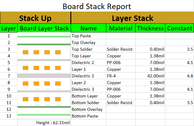
When you’ve finished your PCB and you want to make sure your fabricator understands your design data, including copper weight, make sure you specify this data to your manufacturer. There’s an important point to note here: your Gerber files will not specify your copper thickness. Gerber files are only in 2D, not in 3D. Instead, you should put this information into a stackup table in fabrication drawings, or you should at least generate a board layer stackup report you can send to your fabricator.
Note: when specifying copper thickness to a PCB manufacturer, it is important to consult their design guidelines and provide clear documentation indicating the desired copper weight or thickness for each layer. Communicating directly with the manufacturer and reviewing the specifications before production is crucial to avoid any misunderstandings.
For more information about PCB fabrication and PCB assembly, contact VictoryPCB at 86-755-86339147 or contact us here.


