In printed circuit board (PCB) design, inner layer clearance refers to the spacing or distance between adjacent copper layers within the board. This clearance plays a crucial role in ensuring proper signal integrity, electrical performance, and reliability of the circuit. In this article, we will explore the important of inner layer clearance in PCB design and discuss its impact on overall circuit functionality.
PCB inner layer clearance, also called spacing or gap, is the distance between conductive traces or features on the inner layers of a PCB. It plays a crucial role in ensuring the reliable and efficient operation of the PCB. Here are a few reasons why PCB inner layer clearance is important.
Inner layer clearance ensures proper electrical isolation between adjacent traces, pads, and copper features on the PCB. It helps prevent electrical short circuits and unintended connections that can lead to malfunctioning or damage to the circuit.
Maintaining appropriate clearance between signal traces on the inner layers is critical for preserving signal integrity. By providing sufficient spacing, it minimizes crosstalk and electromagnetic interference (EMI) between neighboring traces, reducing the chances of signal degradation and ensuring accurate data transmission.
Inner layer clearance is particularly important in high-voltage applications. To determine the inner layer clearance of a PCB, the manufacturer must first know the high and working voltages for the circuit board. The working voltage of the circuit board and its corresponding high voltages can vary widely, so the optimum inner layer clearance can be different for different voltages and circuit boards. The IPC-2221 standard defines the rules for PCB inner layer clearances. This standard covers the most critical details of the PCB design, including electrical clearances, board shape, and mounting holes. These parameters will determine the mechanical support and placement of components.
Inner layer clearance can also influence the thermal performance of the PCB. Sufficient spacing between copper features allows for efficient heat dissipation, preventing heat buildup and potential damage to the components or surrounding circuitry.
By maintaining appropriate inner layer clearance, PCB designers have more flexibility in routing traces and placing components on the board. Sufficient spacing provides room for design modifications, component upgrades, and future expansions, enhancing the overall flexibility of the PCB design.
If you’re not interested in learning about the significance of creepage and clearance through personal experience, there are a few standards to help us. The IEC 60601 and IPC 2221 standards are particularly helpful in determining the appropriate spacing between conductors based on different voltage levels and situations. These standards provide specific guidelines to ensure the safety and reliability of electronic designs.
Several documents cover PCB creepage and clearance standards, with the primary one being IPC-2221. This standard provides general guidelines for various design rules, including the required spacing for high voltage circuits. The limits for spacing are determined based on factors such as the voltage type (DC or AC), the layers within the PCB, whether the external layers are coated or uncoated, and the materials used for the substrate. In addition to IPC-2221, you can find additional information in these standards:
IPC-9592: This standard is more specific than IPC-2221 in that it defines spacing requirements of power conversion devices that run higher than 100 volts.
UL-61010-1: These standards specify the requirements for safety in the design of electrical testing and laboratory equipment as well as other industrial equipment.
UL-60950-1: This standard is for high and low voltage applications across a broad range of equipment.
Designing high voltage/high current circuits and high-speed circuits requires adherence to safety requirements and ensuring signal integrity. Two important design aspects that are crucial in both areas are PCB trace clearance and pad clearance values. These design choices play a vital role in achieving a balance between safety, noise suppression, and ease of manufacturing. By carefully considering and implementing appropriate clearance values, designers can ensure the reliable and efficient operation of their circuits while maintaining the necessary safety standards and minimizing signal interference.
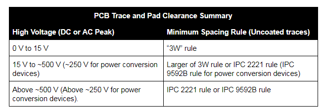
Under the IPC 2221 voltage and spacing standards, the minimum PCB clearance rules (really, the clearance between any two conductors) is 0.1 mm for general-purpose devices or 4 mils. For power conversion devices, this minimum PCB trace with and spacing is 0.13 mm, or 5.1 mils. These boards could hardly be considered “high voltage” and the conductor spacing in these boards starts to border on the HDI regime.
At these voltages, you may be working with digital signals, low-frequency analog signals, or simply DC at moderate current. With digital signals, the typical rule is to simply follow the “3W” rule, where the clearance between traces is triple the width of the trace. For a typical 50 Ohm controlled impedance microstrip, your trace width will be ~20 mils, thus the recommended PCB trace spacing is 60 mils. You’re still well within IPC 2221 requirements with these traces, and your primary focus should be efficient routing and DFM. Even in the HDI regime, where you may need to route between fine-pitch pads in a BGA, you won’t need to worry about these voltage requirements as you’re generally working at 3.3 V or ~1 V.
At high DC voltage, the primary concern in choosing a PCB trace clearance value is preventing ESD and dendritic growth between exposed conductors. With high AC voltage, or with a switching regulator that outputs high current, you now have to worry about crosstalk, as well as ESD and dendritic growth. Crosstalk suppression guidelines still over-specify the required voltage spacing between conductors until you get to very high voltages.
To see how you might need to find a balance between IPC 2221 and crosstalk suppression, consider the following hypothetical situation. Suppose you have a controlled impedance microstrip (20 mil wide) near a high voltage AC line, or near traces running in/out of a high current DC regulator. If you follow the “3W” rule, the spacing between parallel microstrips and the nearby high voltage line should be 1.5 mm, or ~60 mils. This is more than enough to comply with IPC 2221 until the high voltage level reaches 180 V for power conversion devices, or 340 V for other high voltage products.
At high voltage, the concern is not so much a digital edge rate as is the frequency of a high voltage AC line. Any oscillating signal can induce a crosstalk signal in a nearby trace if the traces are close together; this is a known noise problem with high-voltage DC regulators and their downstream signal lines. At high output current, such crosstalk can induce unintended switching in high-speed digital components. It’s best to opt for greater spacing between a high voltage AC line and nearby DC or digital lines.
In summary, PCB inner layer clearance is vital for maintaining electrical isolation, signal integrity, voltage safety, manufacturability, heat dissipation, and design flexibility. By considering these factors and adhering to appropriate clearance guidelines, PCB designers can create reliable and high-performance circuit boards suitable for a wide range of applications.


