When designing a printed circuit board (PCB), understanding the various interconnection options is crucial for successful implementation. Two common interconnection methods are plated through holes (PTHs) and vias. These interconnects play a vital role in establishing electrical connections between different layers of the PCB and components. While both serve similar purposes, there are significant differences between plated through holes and vias that impact their applications and functionality. In this article, we will explore the differences between plated through holes and vias, examining their definitions, construction, purposes, and applications.
| Plated Through Hole (PTH) | Via | |
|---|---|---|
| Definition | A hole with copper plating | An electrical connection between layers |
| Purpose | Provides electrical connection between layers or to components | Establishes electrical connections between layers |
| Construction | Copper plating extends through the entire hole | Copper pad connects the layers through the hole |
| Types | Single-sided, double-sided, and multilayer PTH | Through-hole via, blind via, buried via |
| Component Mounting | Components can be mounted directly into PTHs | Components are not mounted directly into vias |
| Conductivity | High conductivity due to complete copper plating | Conductivity depends on the plating and inner layer connections |
| Size | Larger in diameter to accommodate components | Smaller in diameter for signal routing |
| Application | Suitable for components requiring a strong mechanical connection | Used for interconnecting signal and power traces |
Plated through holes (PTHs) are the most common type of via in a printed circuit board (PCB). They can be easily identified by holding the PCB up to light and checking for visible light passing through the holes. PTHs are relatively simple to create using drills or laser lights to create a complete borehole, making them cost-effective. However, not all circuit layers require plated through holes, and their usage can consume additional PCB space. These holes are drilled through the PCB and lined with a conductive material like copper, which is then plated with metals such as tin or gold. The purpose of PTHs is to establish connections between different PCB layers or components on the board, facilitating the flow of electrical signals.
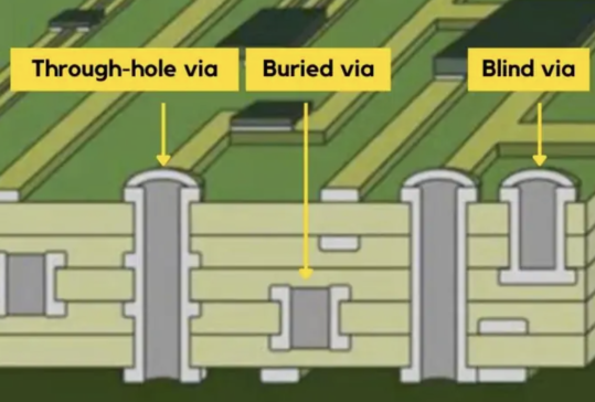
A via is a hole drilled through a single layer of the PCB and filled with a conductive material like copper. Vias are primarily used to establish connections within the same layer of the PCB or to connect components on the same side of the board. They come in two main forms: through-hole vias and microvias. Through-hole vias are larger in diameter and commonly found in standard PCB designs, while microvias are smaller in diameter and used in high-density circuit designs where space is limited. Understanding the distinctions between vias and their different types is crucial for successful PCB layout and design.
When comparing Plated Through-Holes (PTHs) with vias in Printed Circuit Boards, it’s crucial to understand their key roles and distinctions in facilitating vertical electrical connectivity. PTHs are specifically designed to traverse the entire thickness of multilayer PCBs, thereby ensuring components on different layers are interconnected, enhancing the board’s functionality by allowing for complex layer-to-layer connections. In contrast, vias primarily focus on local connectivity, linking electronic components or traces within the same layer or between immediate adjacent layers only. This difference is significant: PTHs serve as the backbone for multi-layer integration and component placement across the entire PCB, while vias provide essential, but localized, connections that support circuit complexity and layer-specific functionality. By leveraging both PTHs and vias, PCB designers can achieve intricate designs and efficient electrical performance, meeting the diverse needs of modern electronic devices.


