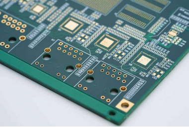
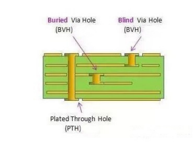
It is a common type of vias, which passes through the entire circuit board and can be used to realize internal interconnection or as a mounting positioning hole for components. Through holes are easier to identify, just hold the PCB up to the light and can see the light passing through holes.

The outermost circuit of the PCB is connected to the adjacent inner layer with a plated hole. Because the opposite side cannot be seen, it is called blind hole. It is located on the top and bottom surfaces of the PCB board, has a certain depth and is used for the connection of the surface circuit and the inner circuit, the depth of the hole usually does not exceed a certain ratio.

It refers to the connection located at any circuit layer inside the PCB but not conducted to the outer layer. This process cannot be achieved by drilling after bonding, drilling must be performed on individual circuit layers. First, the inner layer must be partially bonded and then electroplated before being fully bonded. Compared with through hole and blind hole, it takes more work, so the price is also the most expensive. This process is usually only used on high-density (HDI) circuit boards to increase the available space for other circuit layers.
Both blind holes and buried holes are located in the inner layer of the circuit board. Before lamination, they are completed by through-hole forming process. During the formation of via holes, several inner layers may be overlapped.
Combination technology of Buried, blind, through-hole is also an important way to increase the density of printed circuits. Generally, buried and blind holes are tiny holes. In addition to increasing the number of wiring on the board, buried and blind holes use the nearest inter-layer interconnection, which greatly reduces the number of through holes formed and the isolation plate setting will also greatly reduced, thereby increasing the number of effective wiring and inter-layer interconnections in the board and improving the high-density interconnection.
Buried and blind hole technology has been used more and more in high-density surface. Not only that, it is widely used in large computers, communication equipment as well as in civil and industrial fields. It has also been applied in some thin boards, such as the processing of various PCMCIA, Smard, IC cards, etc., with blind and buried multi-layer PCB circuit boards with more than six layers.