Ensuring the reliability and quality of printed circuit boards relies heavily on solderability testing, which evaluates the ability of PCB components to form robust solder joints. This process can help identify issues like oxidation, contamination, and poor wetting. By detecting these problems early, manufacturers can prevent costly rework and product failures. Solderability testing also ensures compliance with industry regulations and customer expectations. The article will cover various methods of PCB solderability testing, such as the dip and look method and wetting balance analysis, highlighting their importance in producing reliable electronic devices.
PCB solderability testing is a quality assurance process used in electronic manufacturing to evaluate the ability of printed circuit board components to form reliable solder joints. This testing ensures that the solder adheres properly to the component leads and pads, which is essential for the electrical and mechanical integrity of the final product.
The solderability test evaluates the ability of terminals and leads to form reliable connections through soldering. It measures how well metal is wetted by molten solder to ensure secure connections, and determines if components can withstand high temperatures during soldering. Additionally, the test assesses if storage conditions affect the components’ solderability. Understanding solderability tests helps minimize PCB failures and improve product quality. In essence, solderability refers to the molten solder’s capacity to maintain an even, unbroken liquid state during the soldering process.
There are various tests designed to evaluate the solderability of PCBs, each test has unique methodology and applications. Here are the primary types of solderability tests:
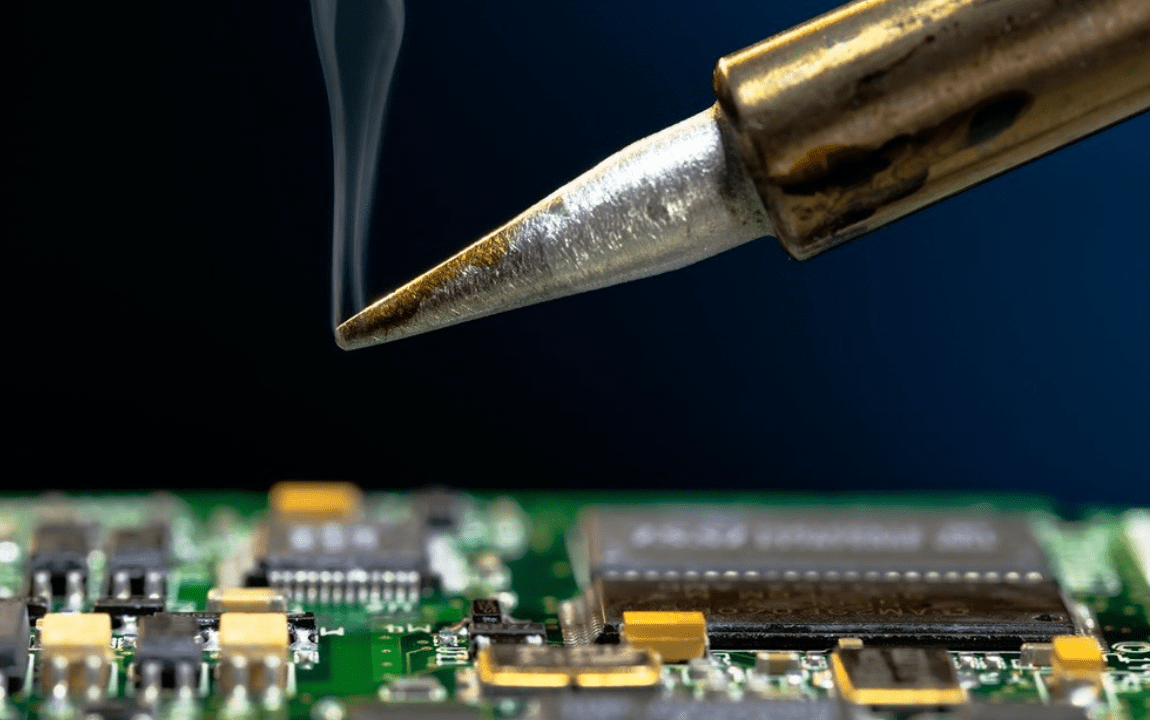
The DIP test is a widely used method for evaluating the solderability of printed circuit boards and component leads. It provides a straightforward and cost-effective way to assess the ability of a surface to form a satisfactory solder joint.
The DIP test evaluates solderability by first cleaning the PCB or component leads and applying flux. The sample is then dipped into a solder bath at 245°C to 255°C for a few seconds using a controlled mechanism. After dipping, the sample cools and any flux residues are cleaned off. The soldered area is then inspected under magnification (10x to 20x) to check for uniform solder coverage and identify defects such as skips, voids, and non-wetting areas.
The DIP test is simple and cost-effective, requiring basic equipment. It provides quick visual feedback, making it useful for rapid assessment. However, its results are subjective and limited to surface observations, lacking detailed quantitative data on solderability metrics. Environmental factors like humidity and contamination can also affect the results.
The Wetting Balance (Meniscograph) test measures solderability by evaluating the wetting forces and time. In this test, a sample is immersed in molten solder using a balance setup that records the wetting force over time. Key parameters measured include wetting force and wetting time, providing quantitative data on how well the solder wets the surface. The resulting wetting curve graphically represents the dynamics of the wetting process.
This test offers precise quantitative data, allowing for detailed analysis and comparison of solderability. However, it requires specialized equipment and expertise, making it more complex and costly than simpler tests like the DIP test. Despite its complexity, the Wetting Balance test is highly valuable for understanding solder behavior and ensuring reliable solder joints.
The Surface Insulation Resistance (SIR) test evaluates the insulation properties of a PCB by measuring the resistance between conductors over time. The test involves applying a voltage across a defined test pattern on the PCB, which is conditioned in an environment simulating real-world conditions, such as high humidity and elevated temperatures. After conditioning, the resistance is measured using a high-impedance meter to ensure the PCB maintains high insulation resistance, preventing electrical leakage and short circuits.
The SIR test is crucial for identifying potential issues like ionic contamination that can lead to decreased insulation resistance and reliability problems. It ensures that the soldering process has not compromised the insulation properties of the PCB, maintaining the integrity of signal paths and preventing failures in electronic circuits. However, the test can be time-consuming, requiring precise equipment and controlled environmental conditions, and interpreting the results may require expert analysis.
Before conducting the solderability test, it is essential to undertake the following preparation steps to ensure accurate and reliable results:
Cleaning and Handling: Thoroughly clean the PCB or component leads to remove contaminants and handle them with care to prevent recontamination.
Selection of Appropriate Test Method: Choose the test method based on the PCB type and production requirements, ensuring compliance with industry standards.
Test Equipment and Tools: Ensure all necessary equipment, such as solder baths, wetting balance testers, and high-impedance meters, are calibrated and ready for use.
With the preparations complete, you can now proceed to do the solderability test with the following 5 steps:
Applying Flux: Apply the appropriate flux to the test area to promote wetting by the molten solder.
Dipping or Immersion: Immerse the sample in the solder bath or wetting balance tester according to the selected test method, ensuring consistent immersion and withdrawal speeds.
Cooling and Cleaning: Allow the sample to cool, typically by air cooling, and then clean off any remaining flux residues using appropriate solvents or cleaning agents.
Measurement and Inspection: Inspect the soldered area under magnification (10x to 20x) or analyze quantitative data from the wetting balance tester to assess solder coverage and wetting properties.
Interpreting Results: Evaluate the test results to identify any solderability issues, such as poor wetting or defects, and take corrective actions as needed.
Identifying and addressing solderability issues is crucial to ensure reliable connections and high-quality PCBs. Here are common solderability issues and how to troubleshoot them.
Poor wetting occurs when the solder does not spread evenly over the PCB pads or component leads, resulting in weak or incomplete joints. This issue is often caused by contaminated surfaces, insufficient flux, or incorrect soldering temperature. To resolve poor wetting, ensure thorough cleaning of the PCB and component leads, apply an adequate amount of flux, and verify that the soldering temperature is within the recommended range. Proper preparation and control of the soldering process are essential to achieve good wetting and reliable solder joints.
Non-wetting happens when the solder fails to adhere to the PCB pads or component leads, leaving exposed surfaces without solder coverage. This issue is typically caused by oxidation of PCB pads or component leads, inappropriate flux, or insufficient heat during soldering. To address non-wetting, clean and deoxidize the surfaces, use flux suitable for the materials, and ensure the soldering process provides adequate heat. Effective cleaning and proper flux application are crucial to preventing non-wetting and ensuring strong solder joints.
De-wetting occurs when the solder initially wets the surface but then retracts, leaving behind an irregular and patchy coating. This issue is often caused by contaminants, poor-quality solder, excessive flux residue, or thermal damage. To resolve de-wetting, use high-purity solder, ensure proper cleaning to remove contaminants and excess flux, and control the soldering temperature to avoid thermal damage. Addressing these factors helps achieve a uniform and reliable solder coating.
In summary, solderability testing helps maintain high-quality standards, reduces defects, and enhances the durability of electronic products. By prioritizing thorough preparation, accurate testing, and continuous improvement, manufacturers can ensure their products meet industry standards and customer expectations.
For reliable and high-quality PCB solutions, consider partnering with VictoryPCB, a leading PCB supplier in China. Contact us now by [email protected] to learn more about our products and services, and how we can help you achieve superior solderability and performance in your electronic components.


