Printed circuit boards are becoming more complex to accommodate higher density components and more complex functionality. The 10-layer PCB is a prime example of this evolution. Designed to handle more sophisticated electronic tasks, it stacks ten individual layers, each serving a unique purpose, into a single, efficient unit. This article will explore the intricate world of 10 layer PCBs, delving into their design, benefits, and challenges. Ideal for those interested in the technological advancements in electronic circuitry, it provides a clear, detailed understanding of these complex components.
A 10-layer PCB is an electronic board featuring ten layers of conductive material for signal routing. This multi-layer structure allows for complex circuit designs, accommodating a denser arrangement of electronic components. You use 10-layer printed circuit boards in applications that need proper electromagnetic conductivity.
The thickness of standard 10-layer Printed Circuit Boards can vary, typically ranging from 1.33mm to 3.0mm. This variation is due to several factors, like the thickness of copper, prepreg (pre-impregnated composite fibers), and core materials used in the PCB. For instance, PCBs that need high isolation might use double layers of prepregs. In situations where the PCB must handle high currents without harming the signal traces, the copper material thickness can be as much as 105um (3oz) or even more. These aspects are crucial in determining the overall thickness of a 10-layer PCB, ensuring it meets the specific needs of its application.
The standard stack-up of a 10-layer Printed Circuit Board is a well-thought-out arrangement that balances signal integrity, power distribution, and grounding needs. This stack-up typically alternates between signal layers and power/ground layers, ensuring efficient circuit operation and minimizing issues like noise and interference.
The typical configuration of a 10-layer PCB includes multiple signal layers interspersed with ground and power layers.
| Layer | Function |
|---|---|
| 1 | Signal |
| GND | Ground Plane |
| 2 | Signal |
| PWR | Power Plane |
| 3 | Signal |
| 4 | Signal |
| 5 | Signal |
| 6 | Signal |
| PWR | Power Plane |
| 7 | Signal |
| GND | Ground Plane |
| 8 | Signal |
| 9 | Signal |
| 10 | Signal |
Top and Bottom Layers: These are generally used for signal routing and are easily accessible for component placement and connections.
Ground Layer: Located just below the top layer, it helps in shielding and reducing electromagnetic interference (EMI).
Alternating Layers: The PCB includes multiple signal layers interspersed with ground and power layers, crucial for maintaining signal integrity, especially in high-speed designs.
Central Power/Ground Plane Pair: This is often included in the middle of the stack-up for better signal referencing, reducing cross-talk and improving performance.
Additional Signal Layers: Placed strategically for complex circuit routing that cannot be accommodated on outer layers. These are positioned considering signal types and noise susceptibility.
Material Selection: Each layer and the prepreg (resin-impregnated fiber) material are chosen based on the electrical and thermal requirements of the PCB.
Prepreg Material: Provides physical stability and electrical insulation between layers.
When designing 10-layer Printed Circuit Boards, here are key points to consider:
Thickness of FR-4 Laminates: For PCBs with more than 6-8 layers, thinner FR-4 laminates, typically between 0.8 and 1.2 mm, are recommended over the standard 1.6 mm. This helps manage the board’s overall thickness for fitting into electronic devices.
Material for High Frequencies: For higher frequency applications, materials with a low dielectric constant (Dk), different from standard FR-4, should be used. These materials improve signal integrity at high frequencies.
Glass Transition Temperature (Tg): The Tg should be over 170°C, especially for lead-free soldering and high-reliability applications. This ensures the material withstands high temperatures without degrading.
Glass Weave Styles: Using tight weave glass styles in laminates ensures more uniform dielectric properties, which is important for consistent electrical performance, particularly in high-speed applications.
The 10-layer Printed Circuit Board offers significant benefits, especially for complex electronic devices. Its layered structure allows for more efficient and sophisticated designs. Here are some key advantages:
More Routing Channels: The ten layers significantly reduce routing congestion, which is particularly beneficial for integrating complex, high pin count Integrated Circuits (ICs). This makes it easier to design intricate circuits without running out of space for connections.
High-Speed Design: The careful stackup of the 10 layers is crucial for maintaining controlled impedance in the lines, especially on the inner layers. This is essential for high-speed electronic designs, ensuring signal integrity and reducing delays.
Smaller Board Sizes: The multi-layered approach allows for a more compact layout, enabling the PCB to fit into smaller enclosures. This is a critical advantage in modern electronics, where there is a continuous push for miniaturization without sacrificing performance.
Higher Component Density: The design accommodates minimal component spacing and reduces footprint size, allowing more components to be placed on the board. This high-density component placement is essential for modern, complex electronic devices.
RF/High-Frequency Design: Additional layers in the PCB assist in controlling losses, parasitics, and providing better shielding, which is crucial for radio frequency (RF) and high-frequency circuit designs.
Mixed Signal Separation: In a 10-layer PCB, digital and analog signals can be isolated on separate layers. This separation is crucial to prevent interference between these two types of signals, ensuring the integrity and accuracy of the data being processed.
While 10-layer PCBs offer several advantages in electronic manufacturing, they also come with a set of disadvantages, especially when compared to simpler PCB designs. Here are some of the main cons associated with 10-layer PCBs:
High Cost: Multi-layer PCBs like the 10-layer variant are more expensive to design, manufacture, and potentially rework. They require more time and labor for assembly, and the complex.
Troubleshooting and Repair Challenges: Repairing a multi-layer PCB like a 10-layer board is more challenging than 2 Layer PCB or 4 layer pcb.
Longer Production Time: This can be a significant factor in projects with tight deadlines or when quick turnarounds are required.
Limited Availability: Not all PCB manufacturers have the capability or equipment to produce multi-layer PCBs.
10-layer PCBs are used in various advanced electronic applications where complexity, performance, and space optimization are crucial. Their multi-layered structure offers enhanced capabilities that are particularly beneficial in the following areas:
In gadgets like smartphones, tablets, and laptops, space is limited but the demand for functionality is high. 10-layer PCBs allow these devices to house more components in a smaller area, enabling them to be powerful yet compact.
Modern vehicles are equipped with advanced systems for navigation, infotainment, and driver assistance. 10-layer PCBs are used in these systems due to their ability to handle complex circuits and withstand the varying environmental conditions within a vehicle.
In medical equipment like MRI machines, patient monitoring systems, and diagnostic tools, precision and reliability are paramount. The 10-layer PCBs offer the necessary complexity and high-density component placement required for these sensitive and crucial devices.
In automated manufacturing and control systems, 10-layer PCBs are used for their ability to support complex circuitry required for sensors, controllers, and actuators. Their reliability and efficiency are essential for the smooth operation of automated processes.
10 Layer Immersion Gold PCB with 1oz Finished Copper Thickness
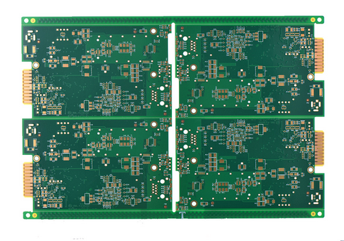
Layer: 10 Layers
Material: FR4 TG170
Dimension: 325.48mm*180.15mm
Finished board thickness: 2.4mm
Outer layer Finished copper thickness: 1oz
Inner layer base copper thickness: 1oz
Surface finishing: Immersion Gold;
10 Layer Immersion Gold PCB with 1.5oz Finished Copper Thickness

Layer: 10 Layers
Material: FR4 TG180
Dimension: 325.48mm*180.15mm
Finished board thickness: 2.0mm
Outer layer Finished copper thickness: 1.5oz
Inner layer base copper thickness: 1oz
Min Trace Width/Space: 3.5mil
Min hole size: 0.2mm
Min hole wall copper: ≥25UM
Soldermask Color: Gloss Green
Surface finishing: Immersion Gold
Choosing the right manufacturer for a 10-layer PCB is crucial to ensure the quality and reliability of your electronic products. Here are some key factors to consider:
Experience and Expertise: Look for a manufacturer with a solid track record in producing multi-layer PCBs.
Manufacturing Capabilities: Ensure the manufacturer has the necessary equipment and technology to produce 10-layer PCBs.
Quality Control Processes: A reliable manufacturer should have stringent quality control measures in place. This includes inspection processes like Automated Optical Inspection (AOI) and X-ray inspection to detect any potential issues with the layers or vias in the PCB. Learn more about PCB Inspection.
Certifications: Look for manufacturers with relevant industry certifications like ISO 9001 or IPC adherence.
Cost-Effectiveness: While cost should not be the only deciding factor, it’s important to ensure that the pricing is competitive and transparent.
If you’re intrigued by the advanced capabilities of 10-layer PCBs and considering them for your next project, Contact us and discuss your specific needs.


