PCB inspection is an essential element in any electronics manufacturing process. Whether for large scale / high volume or low volume manufacturing, the PCB inspection process is essential, especially with the high level of complexity or many of today’s boards.
Here’s an overview of various tips and techniques for PCB assembly inspection.
PCB inspection is the process of visually examining a printed circuit board (PCB) to ensure that it meets the necessary design specifications, quality standards, and functionality requirements. This is done through a series of procedures that have largely become automated.
PCB inspection is a critical step in the manufacturing process because even a small error or defect in the PCB can lead to significant problems in the functioning of the electronic device. After a printed circuit board has been fabricated, an inspection is done to seek out any shorts or defects that might be present before shipping. A second inspection occurs after PCB assembly components have been attached to the board.
Depending on the class of circuit board being produced, more stringent rules around testing must be followed, especailly in medical, aerospace, and military applications, which require an exacting degree of precision from printed circuited boards, and thus have the highest inspection frequency.
In the early days of PCB manufacture, or the manufacture of any electronics equipment, all inspection was undertaken manually. The form of inspection was called MVI, or manual visual inspection. This was the best option, but was recognised as having only limited value.
As the complexity of printed circuit boards has grown exponentially over the years, manual visual inspection has grown out of practice. This method was seen as easily prone to failure thanks to human error, and produced substandard board quality as the complexity of printed circuit boards spiked. When not caught early, defects lead to faulty boards that become increasingly more difficult to fix as the board proceeds down the assembly line, leading to higher costs and greater amounts of waste from faulty boards.
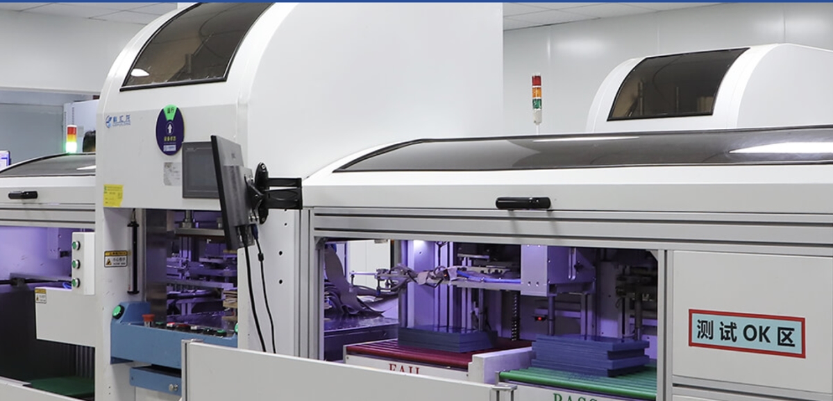
To reduce human error, the visual inspection process has become largely automated. Paired with surface mount technology, inspections can proceed at a much higher rate with greater degrees of accuracy. There are various methods by which PCB inspection can be achieved.
Automated optical inspection is the preferred method of PCB inspection. It utilises an optical system that takes an image of a good assembly and compares the two images to detect any faults or other issues.
It is particularly useful for detecting issues early in printed circuit board manufacturing, such as scratches, nodules, stains, thinning solder, open circuits, and short circuits. AOI systems can also detect incorrect or missing components.
Both two-dimensional and three-dimensional AOI equipment is available. 2D AOI machines use colored lighting from multiple angles and side-angle cameras to inspect components for which height is a factor. 3D AOI equipment is newer and can quickly and accurately measure component height.
AOI is faster than MVI and eliminates the possibility of human error. Like MVI, it can’t be used to inspect components that are out of the line of sight, such as connections that are hidden underneath ball grid arrays (BGAs) and other types of packaging. It might also not be effective for PCBs that have a high concentration of components because some of them may be hidden or shadowed.
With the advent of surface mount technology, or SMT, smaller components have led to more densely populated boards with over 20,000 solder connections. Solder connections on these boards are small enough that they can’t be inspected by AOI equipment. Additionally, multilayered PCBs may contain components that are not visible from the surface. X-ray inspection offers a more comprehensive view of a PCB’s internal structure, providing a more detailed assessment than what can be achieved through surface examination alone.
X-ray inspection is ideal for more complex boards and offers some capabilities that other inspection methods do not, such as the ability to see through chip packages. It also works well for inspecting densely packed PCBs and allows for a more detailed inspection of solder joints. As it is a newer technology in the world of PCB manufacturing, it is expensive to purchase and use, making it unnecessary for lower class printed circuit boards that lack the complexity found in new chip packages. It requires experienced operators to use these machines, and the process can be extremely time consuming, leading to added expenses for customers.
To understand what x-ray PCB inspection is, you first need to know how x-ray inspection works. All x-ray inspection devices are made up of three basic features:
X-ray tube: This tube has the ability to generate x-ray photons.
Platform: The operation platform moves the sample in different directions, allowing it to be inspected from various angles and magnitudes.
Detector: The detector on the other side of the sample catches and collects x-ray photons, converting them into an image.
If the design of your PCB requires a unique form of inspection, VictoryPCB can offer specialized inspection services to meet your needs. Our in-house team of experts knows the importance of quality control and we will work with you to make sure your PCB assembly meets all expectations of performance.
For high volume production these days most manufacturers use AOI systems for their PCB inspection functions. With the increase in the number of BGAs and BGA associated packages being used, AXI is also being increasingly used.
There are two main uses for a PCB inspection system: High light manufacturing defects and Provide process feedback.
The obvious function of a PCB inspection system is to highlight any defects so that they can be corrected before they are passed on to the next stage in the production process. Finding faults as early as possible in the production process is essential because fault finding and fixing costs rise by approximately a factor of ten as each stage in the production process is passed.
An equally important function of a PCB inspection system is to provide feedback into the manufacturing process. Using a PCB inspection system on the output of the soldering process can enable any pattern faults to be seen and the process corrected almost immediately to reduce or eliminate the occurrence of a given problem.
At EMSG, we understand how important the performance of your PCBs is as well as how crucial proper inspection is to ensuring adequate performance. We’re experts in how to implement quality inspection of PCBs. Our team will work with you to determine the ideal printed circuit board inspection criteria and method to use for your project while maintaining acceptable cycle times.
We perform a visual inspection under magnification of every unit we produce and can also provide other inspection services depending on each project’s requirements. We may use AOI to inspect your PCBs optically.
We are certified to ISO 9001:2015, ISO 14001:2015, IATF 16949:2016, ISO13485, SA8000 IECQ QC 080000:2017 and UL certification. ensuring that following exacting guidelines is the only way to ensure success. This means utilizing advanced inspection and testing techniques to ensure only the best results.
Contact us today to learn more about our services.


