In order to improve the quality of your products, it is essential to conduct "appropriate inspections" during manufacturing and "feedback correct information on defects to designers." From the results of this fact-finding survey, we hope that you will be able to understand what kind of board inspection issues production engineers’ face.
Testing a Printed Circuit Board (PCB) is a crucial step in the production process to ensure that the board functions as intended. In this article, we will examine several of the most prevalent PCB testing techniques.
Visual inspection is the most fundamental form of testing and involves visually inspecting the PCB for any defects or anomalies. This can be accomplished manually or using a machine vision system. During this step, the inspector searches for broken or missing components solder bridges, and other issues that are visible to the naked eye.
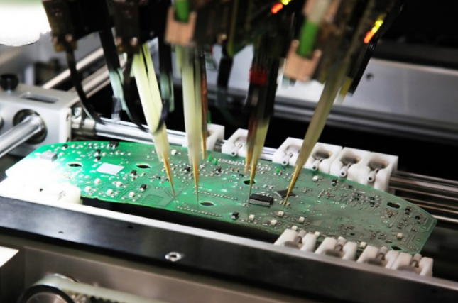
AOI is a machine vision system that utilises cameras and software to detect PCB defects. Invisible to the naked eye, AOI can detect issues such as missing components, misaligned components, and solder defects. AOI systems can inspect PCBs significantly faster than human inspectors and with a high degree of precision.
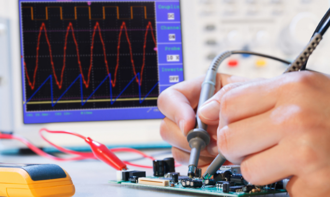
In-Circuit Test (ICT) is a method for testing the functionality of a PCB by making contact with the test points on the PCB using a bed-of-nails test fixture. The ICT system applies a voltage or current to the circuit's test points and measures their response. This method can identify problems such as open circuits, short circuits, and improper component values. ICT is a quick and effective method for testing a PCB's functionality.

Functional testing is the process of evaluating the functionality of a PCB by applying power to the board and observing its performance. This entails connecting the PCB to the appropriate power supply and input/output devices and executing a series of test cases to verify the board's functionality. This method can detect issues that may not be detectable by other testing methods, such as incorrect signal levels, timing issues, and others.
Boundary Scan Testing is a method of testing the digital logic on a PCB. This method involves adding boundary scan cells to the PCB in order to test the interconnections between integrated circuits. Open circuits, short circuits, and stuck-at faults can be identified using the boundary scan cells to test the PCB's connectivity.
The miniaturization of chip parts is progressing more than we imagined due to the availability and cost of parts. First, regarding the size of chip components, , we found that more than 50% of companies use 1005-size chip components. In addition, 47% of companies use chip parts of 0603 or less.
As the chip size becomes smaller, the area on the board becomes smaller, and the board design becomes more accessible. However, various mounting problems, such as mounting defects such as chip standing and cracks during mounting and insufficient solder due to the minor pad size increase. I will come.
It is generally difficult to manually repair parts below 0603, so it is essential to provide feedback to prevent manufacturing defects through post-mounting tests and failure analysis when defects occur. It is a good idea to determine the optimal design rules based on accurate feedback from production engineers.
We had expected that 0.8mm pitch would be the most common, but 0.3 to 0.5mm pitch exceeded 40% and was the most common result. Board designers must be having difficulty figuring out how to pull out the inner pins.
It is known that BGA parts with a pitch of 0.5 mm or less are prone to mounting troubles, so we should consider how to test and guarantee to mount and how to identify failure points during design. You will need to leave.

Inspecting BGA parts by visual inspection and visual inspection is complex, and detecting microcracks by X-ray inspection is challenging. Therefore, electrical testing is the most effective method. Still, if a test pad for inspection is provided on the outer layer, it becomes a stub for high-speed signals and a noise source due to signal reflection.
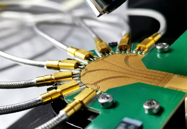
JTAG testing is an electrical test that can handle the BGA component as a test probe, so it is the most suitable inspection method for testing and debugging BGA-mounted boards.
Next, let's compare the 2007 and 2020 fact-finding survey results on printed circuit boards. Regarding changes in the number of pins, the peak in 2007 was 5,000 pins or less, but the peak in 2020 decreased to 1,000 pins or less.
In addition, it was found that the number of nets peaked at 2,000 or less in 2007, but decreased to 1,000 or less in 2020.
Around 2007, industrial equipment was composed of a board that combined a microcomputer and an FPGA, but in 2020, FPGAs with built-in Arm processors became mainstream and became a single chip. It is likely to be on the decline.
There is a tendency to misrepresent non-defective products as non-defective products. As miniaturization and densification progress, what kind of inspection method issues are companies developing products facing?
The survey shows that many companies need help with appearance inspections, visual inspections, and function tests. The decrease in test coverage due to increased BGA parts has become a problem regarding visual inspection and visual inspection. In addition, we found that the increase in delicate chip parts has resulted in smaller fillets for visual inspections.
As for function testing, the development of test programs is becoming more complicated due to product sophistication and single-chip integration, where the processor is built into the FPGA.
In addition to product development resources, securing development resources for mass production testing is becoming difficult. Another problem is the ballooning cost of developing test programs.
Next, regarding the issue of utilizing inspection data, a comparison of 2007 and 2020 shows that although many companies have issues with inspection quality and the number of personnel, minor changes have been observed.
On the other hand, there was a significant change in the number of companies citing inspection costs as an issue. The number of companies citing feedback from the manufacturing department to the design department as an issue increased significantly.
Many companies are considering accumulating and utilizing mass-production inspection data. Still, we have seen a situation where they are worried about how to provide feedback to the design department.
To provide feedback on the design, performing accurate failure analysis on defective products is necessary. However, since failure analysis is complicated for narrow-pitch BGA and delicate chip parts, what kind of inspection method should be used? It seems that you are worried about
What are you doing to prevent the recurrence of manufacturing defects? Data indicates responses from companies with high-density mounting that use delicate chip parts of 0603 or less.
Data in blue indicate responses from companies with medium-to-low density mounting that use chip parts of 1005 or more. As expected, companies using delicate chip parts are more proactive in preventing recurrence.
Many companies collect and analyze inspection data and provide feedback to design. However, we found that efforts for feed forward from design to manufacturing and design for testability (DFT) have yet to progress.
In particular, the idea of design for testability has been appealed to at the Institute of Electronics Packaging since the beginning of 2007. Still, it has not penetrated the design and manufacturing sites. Maximizing test coverage by considering mass production inspections at the design stage improves product quality and reduces manufacturing defects. Why don't you work on "design for testability" as a keyword for the design review?
How do you compare the trends in printed circuit boards and components and issues related to inspection and recurrence prevention introduced this time to your situation? Many companies have similar problems and are working to solve them, so the Inspection Technology Committee holds discussions to solve them and makes various proposals at public research meetings.