Professional PCB Manufacturer

Professional PCB Manufacturer
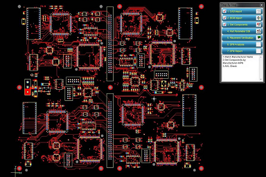
There is no such thing as a standard printed circuit board as each PCB has a single function for a particular product. Producing a PCB is a complex multi-step process. Here, we look at the most important manufacturing steps in producing a multilayer PCB.
The first step in the PCB manufacturing process is design. Designers use specialized software such as Extended Gerber or IX274X to create a blueprint for the PCB that meets all requirements and specifications. These software tools serve not only for layout design but also encode the necessary information for the design output format.
Extended Gerber is a commonly used design software that encodes various information designers need, such as copper layer count, solder mask layer count, and component symbol. Once the PCB blueprint is coded, all design aspects are checked to ensure no errors exist.
The PCB fabrication house receives the completed PCB design for fabrication preparation. At the fabrication plant, the design plan is subjected to design for manufacturing (DFM) checks to ensure that the design meets the tolerances required for the manufacturing process. The purpose of the DFM inspection is to guarantee manufacturability and ensure that the quality of the design is at the best level.
After the DFM check is passed, the designer conducts a design review and resolves possible engineering issues to ensure the accuracy and reliability of the design.
Design reviews and engineering issues are vital in the second step of the PCB manufacturing process. This step checks the design for potential errors or flaws and ensures a smooth manufacturing process.
Engineers conduct design reviews and scrutinize every part of the PCB design to ensure all components and correct structures are included. They also verify that the design meets the required specifications and does not violate manufacturing guidelines. Only after the engineer approves the design does the next stage - printing.
After all the checks are done, printing the PCB design is the next step. Unlike other plans (such as architectural drawings), PCB designs are not printed directly on regular 8.5 x 11 paper. Instead, a special printer, called a plotter, is used to make a "film" of the PCB. These "films" are actually negatives of the PCB itself, similar to the transparencies commonly found in schools.
The inner layers of the PCB are represented using two ink colors: black ink is used to show the copper traces and circuits of the PCB, while clear ink represents non-conductive areas such as the fiberglass base. On the outer layers of the PCB design, however, this representation is reversed—clear ink refers to copper via lines, while black ink indicates areas of copper that will be removed.
Each PCB layer and corresponding solder mask layer has its own film, so a simple two-layer PCB requires four sheets—one for each layer and two accompanying solder mask sheets.
After the films have been printed, they need to be lined up and punched with a hole punch, also known as a pilot hole, in them. These alignment holes serve as reference points for aligning the film during subsequent fabrication.
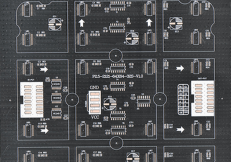
Step four marks the beginning of creating the PCB. The process begins by printing the PCB design onto a special material called laminate. Then, a layer of copper foil or copper coating is applied to the laminate. The copper is firmly attached to the laminate, forming the structure of the PCB. Then, excess copper is removed to reveal the desired design.
Next, a photosensitive film called resist is applied to cover the laminate. Resists, which contain special chemicals that harden under ultraviolet light (UV), enable technicians to match the PCB design and the photoresist perfectly.
To align the resist accurately, technicians use holes created earlier in the process. The laminate and resist are then exposed to UV light. UV light passes through the transparent portion of the film, hardening the photoresist. This indicates areas where copper should remain, forming channels. Meanwhile, the black ink on the resist prevents UV rays from reaching areas that shouldn't harden, making them easier to remove later.
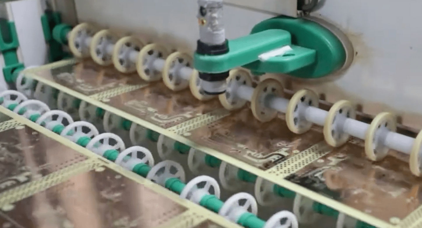
Once the board is ready, it is cleaned with an alkaline solution to remove any residual photoresist. This is followed by a thorough pressure wash to ensure a clean surface. Leave the plate to dry.
After drying, the only remaining resist should be on top of the copper that will be part of the final PCB. A technician double checks the PCB for any errors. If everything looks good, the process goes to the next step.
This important process lays the foundation for a multilayer PCB, precisely defining its electrical connections. Precision here ensures that the PCB will perform correctly and reliably in its intended application.
This step is all about carefully removing extra copper from the inner layers of the PCB to reveal the copper traces that match the PCB layout design.
During etching, the core or inner layers of the PCB undergo a chemical treatment. The necessary copper on the board is covered and protected, while the rest of the board is exposed to a special chemical. This chemical process skillfully removes all the unprotected copper, leaving only the precise amount of copper needed for the PCB's functionality.
The time and amount of copper etching solvent used may vary depending on the PCB's size and structure. For larger PCBs or those with heavier structures, more copper might be used, requiring additional time or solvent for the etching process.
So, etching plays a vital role in perfecting the PCB's copper traces, ensuring they match the design layout accurately and guaranteeing the board's optimal performance.
Layer alignment is a critical step in the manufacturing process of a multilayer PCB. Once the individual inner copper layers of the PCB have been created, they need to be carefully aligned and bonded together to form a complete and functional multilayer PCB.
During the layer alignment process, each inner copper layer is precisely positioned and bonded to the adjacent layers. This alignment ensures that the electrical connections and vias (holes connecting the layers) between the layers are accurately aligned, creating a continuous and reliable conductive pathway throughout the PCB.
Technicians use alignment tools and registration marks on the copper layers to ensure the proper positioning. These registration marks act as reference points to help match the copper layers correctly. The layers are then laminated together under heat and pressure, permanently bonding them to form a solid multilayer PCB.
Small holes called vias are drilled through the PCB to connect different layers electrically. Larger holes are also drilled for component mounting.
Before drilling, an X-ray machine is used to locate the drill spots. Then, registration/guiding holes are drilled so that the PCB stack can be secured before the more specific holes are drilled. When it comes time to drill these holes, a computer-guided drill is used to make the holes themselves, using the file from the Extended Gerber design as a guide.
Once the PCB panel has been drilled, the next crucial step is plating. During this process, a series of chemical treatments are used to fuse all the different layers of the PCB together. The PCB is thoroughly cleaned and then bathed in chemicals, resulting in the deposition of a micron-thick layer of copper.
This copper layer coats the top-most layer of the PCB and fills the holes that were just drilled. Before the plating, these holes exposed the fiberglass substrate inside the panel. However, after the plating, the holes are now lined with copper, effectively covering their walls.
Earlier in the process (Step Four), a photoresist was applied to the PCB panel. In this step, we apply photoresist to the outer layers of the panel and expose them to UV light to create the PCB design. The yellow room prevents UV light from affecting the photoresist. Black ink transparencies ensure precise alignment during exposure to high UV light, hardening the photoresist.
The outer plates undergo inspection to ensure all unwanted photoresist is removed. Later, we apply another layer of photoresist to the outside layer for imaging. The outer layers are then plated in the same way as the interior layers, with the addition of a tin plating for extra protection.
During the final etching of the outer layer, the tin guard shields the valuable copper, ensuring it remains protected. Unwanted copper is removed using the same copper solvent, while the tin preserves the desired copper in the etching area.
Unlike the inner layer, the inks are reversed for the outer layer. Dark ink covers non-conductive areas, and light ink is applied to the copper, allowing tin plating to protect it. Engineers remove any unnecessary copper and remaining resist coating during etching, preparing the outer layer for automated optical inspection (AOI) and solder masking.
AOI checks ensure the layer meets design requirements and verifies that all excess copper is removed, resulting in a fully functional printed circuit board with proper electrical connections.
In preparation for solder mask application, panels undergo a thorough cleaning. An epoxy solder mask ink is then applied to cover the board's surface. Ultraviolet light is used to indicate areas where the solder mask should be removed.
After technicians remove the designated solder mask, the circuit board goes into an oven for curing. This mask provides valuable protection to the board's copper, shielding it from potential damage caused by corrosion and oxidation.
In the PCB fabrication process, important information is printed on the board's surface through silkscreen application or legend printing. This includes company ID numbers, warning labels, manufacturers' marks, part numbers, and other marks. After printing this data and applying the surface finish, the PCBs undergo testing, cutting, and inspection.
To enhance solder-ability, some PCBs receive chemical plating with gold or silver, and hot air leveling is used to create uniform pads. This generates the surface finish, which can be customized based on customer requirements.
The nearly completed PCB is then ink-jet written with vital information. Finally, it goes through the last coating and curing stage. These steps ensure a fully functional and well-labeled printed circuit board ready for its intended use.
After PCB fabrication, technicians conduct electrical tests to ensure functionality and conformity to the original design. The electrical testing follows IPC-9252 standards and includes circuit continuity and isolation tests. The continuity test checks for disconnections ("opens"), while the isolation test verifies if there are any shorts in different parts of the PCB. These tests not only guarantee functionality but also assess how well the initial PCB design withstands the manufacturing process.
Additionally, the "bed of nails" test is used to determine PCB functionality. This involves attaching spring fixtures to test points and subjecting them to high-pressure contact to evaluate the board's durability under such conditions. These comprehensive electrical assessments ensure the PCB's quality and reliability.
In the final steps of PCB fabrication, profiling and cutting are crucial. Profiling involves identifying the shape and size of individual PCBs from the construction board, using information from Gerber files. This guides the routing out process, where a router or CNC machine creates small pieces along the edges of the board for easy separation without damage.
Alternatively, some fabricators use a v-groove machine to create diagonal cuts along the sides of the board. Both methods ensure clean separation without cracking. After scoring the boards, they are broken from the construction board, completing this stage.
In the last step, cutting, different boards are separated from the original panel using either a router or a v-groove. The router leaves small tabs along the board edges, while the v-groove creates diagonal channels. Both methods allow the boards to easily pop out from the panel, finalizing the fabrication process.
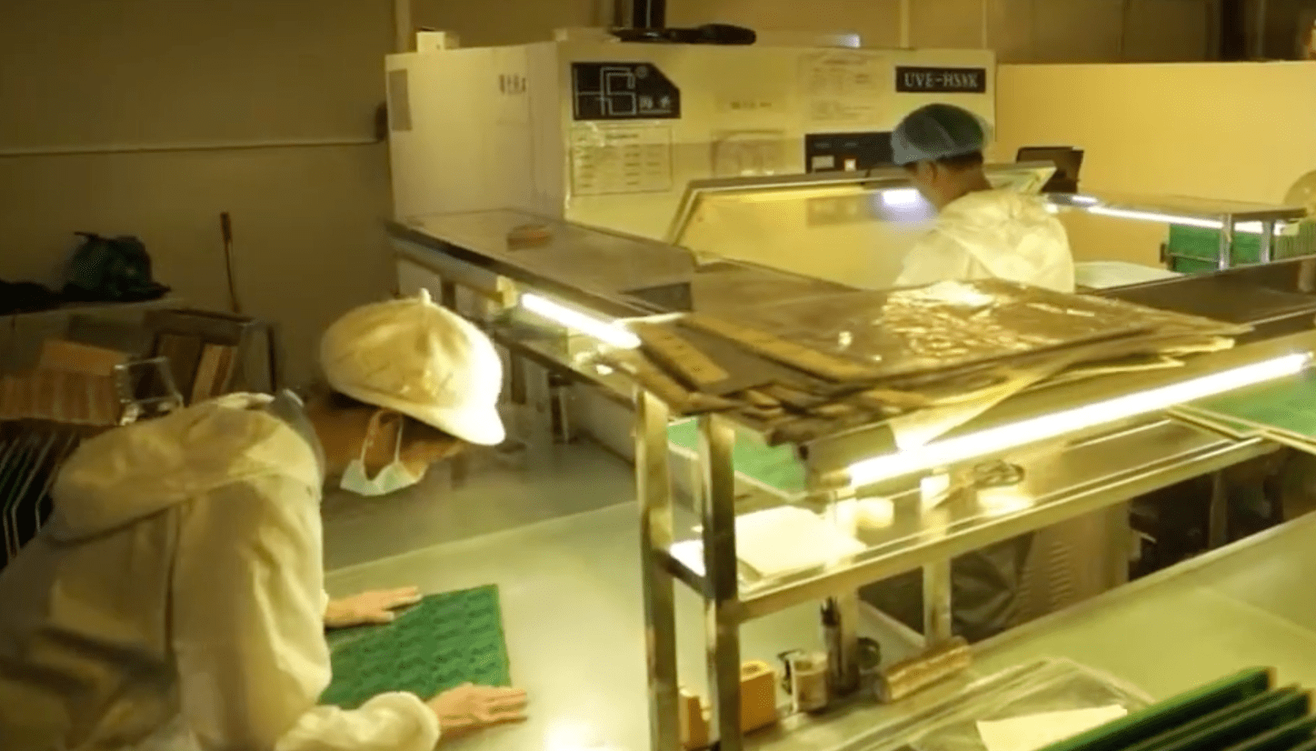
In the last step of the process, a team of precision sight inspectors give each plate a delicate added check. Visually checking the PCB against acceptance existing standards.
Note: Ensure that you liaise with a leading PCB manufacturer that has state-of-the-art equipment.
Achieving a top-notch circuit board manufacturing necessitates a strong collaboration between your PCB contract manufacturer and the chosen fabrication vendor responsible for building the bare boards. For the desired level of fabrication quality, VictoryPCB sets specific criteria that a fabrication vendor must meet to be deemed qualified and suitable for the project.
We are certified to ISO 9001:2015, ISO 14001:2015, IATF 16949:2016, IECQ QC 080000:2017 and UL certification.
We can manufacture 1-16L layer Rigid PCBs, Flex PCBs, High Frequency PCBs, HDI PCBs and Metal Base Aluminium PCBs to satisfy various demand from customers.
We have advanced PCB production and testing equipments to make sure the stable and excellent quality of the production process to meet customer’s requirements.
We are competitive on cost while achieving 100% on-time deliveries.
If you’re looking for the best quality PCB fabrication company, Contact us and get a quote for PCB fabrication now.


By continuing to use the site you agree to our privacy policy Terms and Conditions.
Recruit global agents and distributors Join us


