After fabricating a pcb, the copper traces on the board are vulnerable to oxidation and corrosion when exposed to the environment. To enhance the lifespan of the PCB and protect the copper traces, a protective coating called a solder mask layer is applied. In this article, we delve into the world of PCB solder masks, exploring their importance, applications, and the key benefits they bring to the PCB manufacturing process.
Solder mask is a protective layer applied to a printed circuit board. It is typically a thin coating of polymer material that covers the copper traces and prevents solder from adhering to areas where it is not intended. The solder mask protects the PCB from environmental influences such as dust and several other contaminants that may lead to shorts in the long run.
There are four main types of solder masks commonly used in PCB manufacturing such as Epoxy Liquid, Liquid Photoimageable, Dry Film Photoimageable, Top and Bottom side Masks.
A topside solder mask allows the electronic engineer to identify the openings in the green solder mask layer already added to the PCB by one of the epoxy, ink or film techniques. Component pins can then be soldered onto the board using those identified places. The pattern of conductive traces on the topside of the circuit board is called top traces and the bottom-side mask specifies openings on the lower surface.
Epoxy liquid solder masks are a most cost-effective and commonly used type of solder mask in the PCB industry. They are applied to PCBs using a silkscreening process. Silkscreening involves using a mesh screen with ink-blocking patterns to transfer the solder mask ink onto the PCB, leaving behind the desired solder mask pattern.
Once applied, epoxy liquid solder masks undergo a curing process. This can involve thermal curing, where the PCB is subjected to heat to initiate a chemical reaction in the epoxy. The heat causes the epoxy to crosslink and harden, creating a protective and insulating layer over the PCB traces. In some cases, UV light exposure may also be used as part of the curing process, depending on the specific formulation of the epoxy solder mask.
Liquid Photoimageable (LPI) solder masks are a popular choice in the PCB industry due to their unique characteristics and cost-effectiveness. LPI solder masks consist of two separate liquid components that are mixed together just before application. This ensures a longer shelf life for the materials, as keeping them separate prevents premature curing or degradation.
LPI solder masks can be applied using different methods, including curtain coating, screen printing, and spray applications. These masks are formulated by combining various polymers and solvents, resulting in a blend that can form a thin coating adhering to the surface of the target area on the PCB. One notable advantage of LPI solder masks is that they often eliminate the need for additional surface finishes, which can save time and costs during the PCB manufacturing process.
Unlike conventional epoxy inks, LPI solder masks are sensitive to UV light. After applying the mask to the PCB, a short “tack cure cycle” is performed to partially cure the mask. Subsequently, the panel is exposed to UV light using either a UV laser or a photolithography process. This exposure to UV light further cures the LPI mask, making it durable and resistant to etchants and solvents.
Before mask application, the panels are subjected to cleaning and are checked for any sign of oxidation. This is done using a chemical solution, aluminum oxide solution, or using suspended pumice to scrub the panels.
Dry film solder mask is a pre-fabricated film applied to the surface of printed circuit boards to protect specific areas during soldering. It is made of a photosensitive polymer material and is laminated onto the PCB, exposing it to UV light to define the desired pattern. The remaining solder mask pattern prevents solder bridging and protects the PCB. Dry film solder mask offers uniformity, precise resolution, good adhesion, chemical resistance, and thermal stability. It is compatible with various fabrication processes and contributes to the reliability and durability of PCBs.
The choice of solder mask depends on factors such as the application requirements, manufacturing process, and desired performance characteristics of the PCB.
Most boards have a epoxy-ink soldermask printed onto each side to protect the copper surface and prevent solder shorting between components during assembly.
The panels are first cleaned and brushed to remove any surface tarnish and then are conveyored into the yellow room.
Each panel is given a final clean to remove any dust from the surface and loaded into the vertical coater. The coating machine simultaneously covers both sides of the panel with the epoxy soldermask ink. The double action ensures that the ink completely encapsulates the copper tracking, typically now 35 — 40 microns higher than the surface of the panel.
Source: https://www.youtube.com/watch?v=bjhBa7VdTEM
When designing a PCB, it’s crucial to follow certain guidelines to ensure the solder mask is applied correctly and functions as intended. Here are some general solder mask design guidelines:
Clearance Specifications: Define a sufficient gap between the solder mask openings and the adjacent pads or traces. This gap, known as clearance, should be at least 0.2mm or more, depending on the registration accuracy of the manufacturing process, to prevent any potential short circuits.
Consistent Clearance: Ensure that the clearance around the pads is uniform. Inconsistent clearance can lead to shorts if the solder mask encroaches too close to the pads or traces in some areas.
Acute Angle Avoidance: Steer clear of sharp angles between the solder mask and the pads. Sharp angles can cause the solder mask to peel away from the board during thermal cycling, which can lead to exposed traces and potential failure points.
Aperture Sizing: Size the mask apertures correctly to allow for the right amount of solder paste during assembly. A common practice is to have a solder mask dam (the space between two openings) of about 0.1mm to ensure proper solder paste deposition.
Fiducial Marks: Include fiducial marks on both the copper layers and the solder mask layers. These marks are essential for aligning the layers during the manufacturing process and for placing components during assembly.
Minimum Track/Space Rules: Be aware of the minimum track and space rules, which are dictated by the resolution limits of the solder mask process. Adhering to these rules ensures that the mask can be applied without bridging between closely spaced traces.
Prevention of Oxidation: Solder mask acts as a protective barrier that prevents the copper traces on the PCB from oxidizing. Exposure to air and moisture can lead to oxidation of the copper, which can deteriorate the electrical conductivity and affect the overall performance of the PCB. The solder mask layer shields the copper traces from these environmental factors, ensuring their long-term reliability.
Prevention of Unwanted Connections: The use of special PCB interconnectors, such as vias and through-hole plating, is common to establish connections between different layers of a PCB. Solder mask plays a vital role in preventing unintended connections between these layers. By covering the non-intended areas, the solder mask prevents solder from bridging or creating unwanted electrical connections, ensuring the integrity of the circuit design.
Dust and Dirt Protection: The solder mask layer provides a physical barrier that helps to keep dust, dirt, and other contaminants away from the electrical connections and the PCB substrate. These contaminants can cause short circuits, signal interference, or degradation of the electrical performance of the PCB. The solder mask acts as a protective shield, maintaining the cleanliness and reliability of the PCB.
Prevention of Corrosion: Solder mask also helps to prevent the electrical connections from corroding. Exposure to moisture or corrosive environments can lead to the formation of corrosion on exposed metal surfaces. The solder mask acts as a barrier, protecting the underlying copper traces and solder joints from corrosion, thereby ensuring the long-term functionality and reliability of the PCB.
The specific thickness requirements for solder mask can vary depend on the specific PCB design, manufacturing process, and industry standards. Here are some additional points to consider:
The minimum acceptable solder mask thickness is often specified by industry standards or the PCB manufacturer. In general, the minimum thickness for solder mask application is around 0.3 mils (7.6 micrometers) or less. Thinner solder mask layers are typically applied near the edges of traces or in areas with tight spacing between components or traces.
While a minimum thickness is defined, it’s generally recommended to have a slightly thicker solder mask layer to ensure adequate coverage and protection. A typical guideline is to aim for approximately 0.5 mils (12.7 micrometers) of solder mask over the traces. This provides a sufficient layer for insulation, protection, and solder bridge prevention.
The thickness of solder mask can vary across the PCB, especially in areas with complex geometries, fine traces, or high-density components. The thickness may be influenced by factors such as the application method (e.g., screen printing, curtain coating, or spray application) and the specific solder mask material used.
PCB solder masks are available in a variety of colors and finishes, providing flexibility in design and customization. The choice of solder mask color and finish can have both functional and aesthetic implications. Here are some common options that VictoryPCB provide:
Glossy Finish
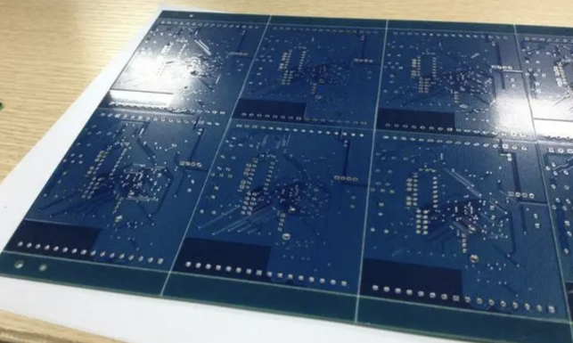
green
black
red
yellow
white
pink
orange
purle
blue
Matte Finish
green
black
white
blue
VictoryPCB is a professional pcb manufacturer to fabricate your PCBs with solder mask with the highest quality to meet your demands. If you have any questions, please feel free to contact us with [email protected], we will be happy to help you.


