The silkscreen layer on a printed circuit board is an essential component of electronic manufacturing, providing crucial information for the assembly, testing, and maintenance of electronic devices. But What Is silkscreen on a PCB and how important silkscreen is in your PCB fabrication? This article delves into the intricacies of PCB silkscreen, exploring its definition, processes, methods, and best practices, thereby illuminating its significance in the seamless integration and operation of electronic components within a vast array of devices.
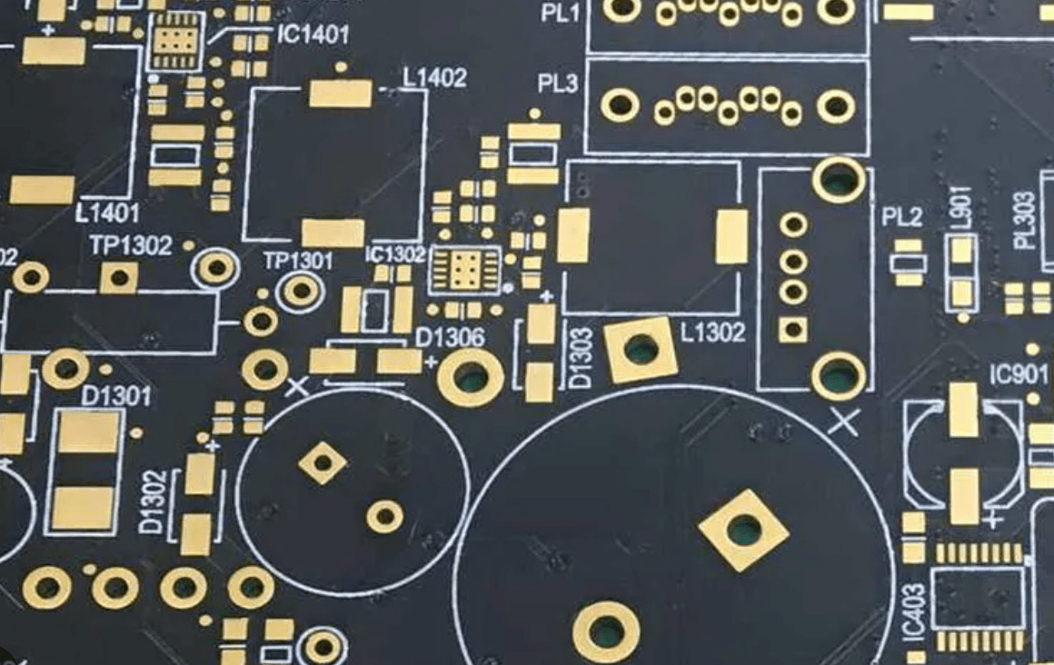
A silkscreen on a PCB refers to the layer of text and symbols printed onto the board’s surface, which provides essential information about the components mounted on it. This includes, but is not limited to, component outlines, identifiers (such as reference designators), polarity markings, test points, warning symbols, and sometimes logos or branding information.
The purpose of the silkscreen is to facilitate the assembly process, help with troubleshooting during testing and repairs, and enhance the overall usability of the PCB by making it easier to understand and navigate. The silkscreen can be applied on one or both sides of the PCB, depending on the complexity of the design and the requirements of the assembly process. The information it contains is crucial for correctly placing and soldering components, ensuring that the electronic device functions as intended.
PCB silkscreen colors can vary, with common choices including black, white, red, blue, and yellow. The selection often depends on the background color of the PCB and the requirements for contrast and legibility.
The PCB silkscreen process is an integral part of PCB manufacturing, providing critical information for component placement, identification, and assembly guidance. Here’s an overview of how the silkscreen process typically unfolds:
The first step involves preparing the silkscreen design, which includes all the text, symbols, and markings that need to be printed on the PCB. This is usually done using PCB design software, where the designer specifies the location, size, and information of each marking.
There are several methods for applying the silkscreen to a PCB, including traditional screen printing, Liquid Photo-Imaging (LPI), and Direct Legend Printing (DLP). The choice of method depends on factors like the complexity of the design, required precision, and production volume.
Screen Printing: This is the traditional method where ink is pushed through a stencil or mesh screen onto the PCB surface. It’s suitable for larger text and images but may lack precision for fine details.
Liquid Photo-Imaging (LPI): LPI is more precise than screen printing and is used for high-density PCBs where fine details are crucial. In this method, a photosensitive ink is applied to the PCB and then developed using UV light, similar to the process for applying a solder mask.
Direct Legend Printing (DLP): DLP uses inkjet technology to directly apply the silkscreen onto the PCB without the need for stencils. This method offers high precision and flexibility for changes late in the design process.
For screen printing and LPI, the ink is applied over the stencil or through the photosensitive process, respectively. In DLP, the inkjet printer applies the ink directly based on the digital design files.
After the ink is applied, the PCB undergoes a curing process, where the ink is dried and hardened to ensure it adheres well to the PCB surface and is durable enough to withstand handling and soldering processes.
The final step involves inspecting the silkscreen for clarity, accuracy, and legibility. This ensures that all markings are correctly applied and that the PCB is ready for the next stages of production.
Designing for silkscreen on PCBs effectively communicates essential information and ensures readability and manufacturability. Here’s an enhanced approach with specific data:
To ensure your text is easy to read, especially at smaller sizes, opt for clear and simple fonts. Sans-serif fonts, such as Arial or Helvetica, are excellent choices. For best legibility, keep your minimum font size at least 0.050 inches. However, to account for any changes during manufacturing, avoid going smaller than 0.035 inches to ensure your text remains clear.
Place text and symbols close to the corresponding components without overlapping pads or traces. Keep text orientation consistent, typically aligned with the board’s major axis, to facilitate easy reading during assembly and troubleshooting.
Use universally recognized symbols and abbreviations to convey information compactly and clearly. Adhere to industry-standard symbols for polarity, ground, and other common elements to avoid confusion.
Keep at least 0.015 inches between text elements and other board features to enhance clarity and prevent overlap. Focus on essential details, such as component identifiers and polarity, to maintain a clean and informative silkscreen layer.
Select a silkscreen ink color offering high contrast against the solder mask color for readability, typically white on green or black on blue PCBs.
Revision Markings: Include revision numbers or letters prominently on the PCB, facilitating easy identification of the board version.
Update Regularly: Ensure that the silkscreen reflects the latest design revisions and component updates.
Component Polarity and Orientation: Clearly indicate component polarity and orientation, using symbols like “+” for positive or an arrow for diode direction.
Test Points and Inspection Marks: Designate test points and include fiducial marks if needed, with test points marked with a diameter of at least 0.040 inches for visibility and access.
Adhering to these detailed best practices in silkscreen design not only improves the PCB assembly process but also enhances the functionality and serviceability of the final product. It’s crucial for designers to integrate these considerations early in the design phase to ensure a smooth transition from prototype to production.
Quality control in the PCB silkscreen process is a critical step to ensure the accuracy, legibility, and overall quality of the printed information on the circuit board. Once the silkscreen has been applied, each board undergoes a detailed inspection phase. This phase is designed to verify that all text, symbols, and markings are correctly and clearly printed in accordance with the design specifications. The goals of this inspection include:
Verifying Legibility: Inspectors ensure that all silkscreened text and symbols are readable and clear, with no smudging, blurring, or partial printing that could lead to misinterpretation during assembly or maintenance.
Accuracy Check: The content of the silkscreen is checked against the PCB design files to confirm that all markings are present and correctly placed. This includes checking component identifiers, polarity markings, test points, and any other critical information.
Adherence to Standards: The inspection also involves ensuring that the silkscreen adheres to industry standards for font size, line width, and spacing, as well as specific manufacturing guidelines. For example, text should be a minimum size (often recommended to be no smaller than 0.035 inches) and placed at a safe distance from component pads and traces to avoid interference during soldering.
Physical Inspection: Beyond the information content, the physical quality of the silkscreen layer is assessed. This includes checking for any defects in the ink coverage, such as peeling, cracking, or inconsistency in thickness, which could impact the durability of the markings.
Advancements in PCB silkscreen techniques and materials have significantly enhanced the precision, durability, and functionality of circuit board markings. With the advent of Laser Direct Imaging (LDI) and inkjet printing, manufacturers can now achieve unparalleled detail and adaptability in design, catering to the demands of high-density component layouts. Concurrently, the development of epoxy and UV-curable inks has ensured that these crucial markings withstand environmental stressors and remain legible throughout the PCB’s lifespan. These innovations not only streamline the manufacturing process but also bolster the reliability and performance of the final products in various applications.
The PCB silkscreen, while often overlooked, is a critical component of electronic manufacturing, offering a blend of guidance, functionality, and even branding on a tiny piece of real estate. As technology progresses, the methods and materials used in silkscreening continue to evolve, promising even greater advancements in the field of PCB design and manufacturing.


