Have you ever wondered how modern electronics can be so compact yet powerful? The answer often lies in microvias, tiny holes that connect different layers within a printed circuit board. These small structures enable high-density interconnect designs, allowing more functionality in a smaller space. As electronics become more complex, microvias are essential for creating efficient, reliable connections in advanced PCB designs. In this article, we will explore the importance of microvias in PCB design, how they enhance performance and reliability, and the considerations for using them in advanced electronic products.
According to the Institute of Printed Circuit Boards (IPC), A microvia hole is a tiny, laser-drilled hole in a printed circuit board with a 1:1 aspect ratio, used to connect different layers, and has a depth of no more than 0.010 inches or 0.25 mm.
The aspect ratio of these vias can be 0.75:1 or even as high as 2:1, but they bring reliability concerns. Because of this, they typically only span a single layer. Note that a microvia aspect ratio that is greater than 1 does not meet the IPC definition of a microvia.
Microvias are crucial in modern PCB design due to the increasing complexity and miniaturization of electronic products, which demand higher density circuit boards with finer tracks and gaps. This leads to a greater number of smaller diameter holes, where traditional plated through via holes are no longer feasible. Microvias, being laser-drilled and smaller than mechanically drilled holes, connect selected layers without passing through all layers, addressing these challenges. Additionally, microvias offer space efficiency, enhanced electrical performance, greater design flexibility, improved reliability, cost efficiency, and support the development of high-density interconnect (HDI) PCBs, making them essential for advanced electronic devices.
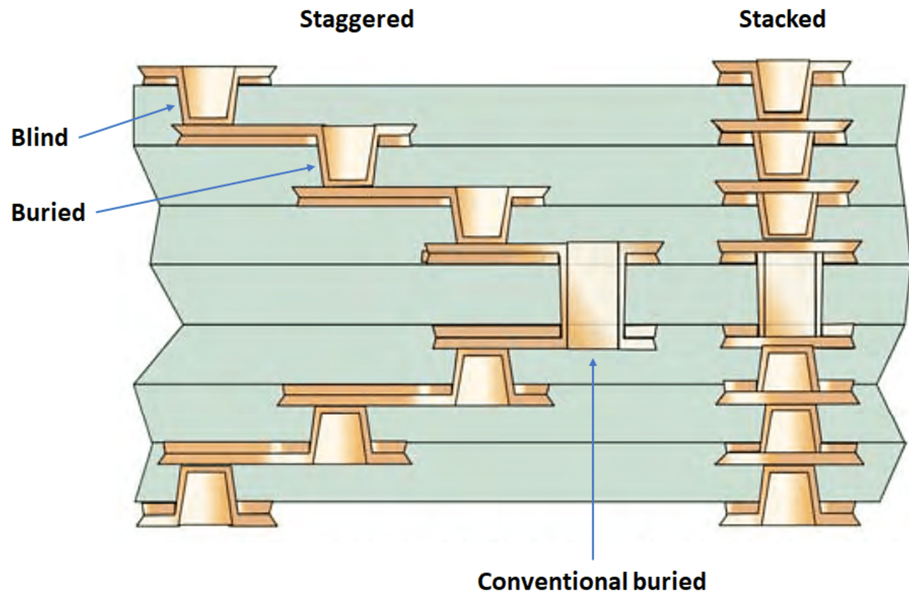
Blind vias connect an outer layer of the PCB to one or more inner layers without passing through the entire board like a through-hole. They are commonly used in HDI designs to increase component density on the surface. This allows for more efficient use of space while maintaining the overall board thickness.
Buried vias connect internal layers of the PCB without reaching the outer surfaces. They are used to enhance the routing density within the inner layers, leaving the outer layers free for additional components or routing. This type of via is essential in multi-layer boards where internal layer connectivity is crucial.
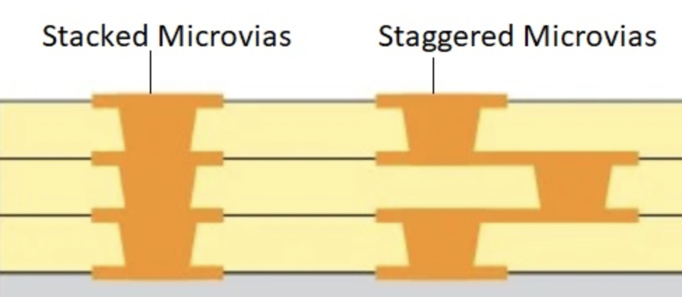
Stacked microvias involve multiple blind and or buried microvias placed on top of each other to connect several layers of the PCB. This technique is used in complex HDI designs to achieve high interconnectivity in a compact area. Stacked microvias are crucial for advanced electronic devices requiring multiple layer connections.
Staggered microvias are microvias that are offset from each other across adjacent layers, rather than being vertically aligned. This placement distributes mechanical stress more evenly across the PCB, enhancing its structural integrity and reliability. Staggered microvias provide greater design flexibility in complex, multi-layer PCBs by allowing for more efficient routing and optimized space usage. This technique is particularly beneficial in HDI designs where maintaining both performance and durability is crucial.
Via-in-pad microvias are placed directly beneath component pads and are often filled and plated over to create a flat surface. This technique maximizes space usage on the PCB surface, allowing for more compact component placement. Via-in-pad is essential in HDI designs to improve board performance and density.
In PCB design, the decision to fill or leave microvias unfilled depends on their application and the specific requirements of the design. Filled microvias are essential for buried microvias and in-pad blind microvias. Buried microvias, which connect internal layers, need to be filled with copper to prevent voids that can cause high stress concentrations along the via walls, potentially leading to fractures during thermal cycles such as reflow soldering. The filling process typically involves conformal plating, followed by pulsed plating to ensure the via body is solidly filled with copper, eliminating voids and ensuring even copper distribution. Additives in the copper or resin are used to achieve uniform plating, further enhancing the structural integrity and reliability of the vias.
On the other hand, blind microvias, which connect an outer layer to one or more inner layers, can sometimes be left unfilled, particularly if they are not used in critical areas like component pads. In the early days of microvia technology, leaving blind microvias unfilled was common practice. However, when blind microvias are used within a pad (via-in-pad), they should be filled to provide a flat and reliable surface for component placement, ensuring better performance and durability. While unfilled microvias may still be used in less critical applications, modern high-reliability designs increasingly prefer filled microvias to maximize the PCB’s performance and longevity.
Staggered vias are more complex to design but are less costly to manufacture than stacked vias, which require more precision and accuracy checks. For reliability, it is recommended that stacked microvia structures be limited to two layers. If a design requires a third layer of microvias, it should be staggered to enhance structural integrity and reduce the risk of failure.
Microvias offer PCB designers flexibility and reliability when connecting multiple layers, making them essential for advanced electronic designs. Selecting the right materials for printed circuit boards is crucial, as some are better suited for the microvia drilling process. Consulting with a PCB fabricator before choosing materials helps ensure the best options for your application.
VictoryPCB is a professional PCB manufacturer with extensive experience in microvia technology. Our team can guide you in selecting suitable materials and optimizing your design to reduce costs and improve performance. Contact VictoryPCB today by [email protected] to discuss your project needs and discover how our expertise can help you achieve high-quality, cost-effective PCB solutions.


