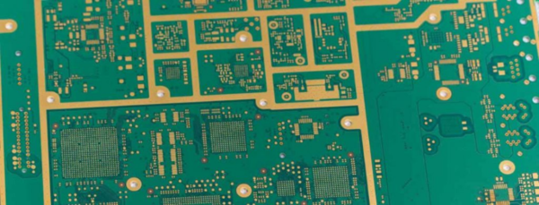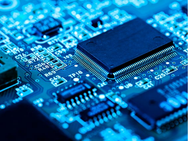
The layer structure of a printed circuit board is defined by how and how many layers are arranged, considering the insulating layer and the layer with copper foil as one layer.
A single-sided PCB contains one layer, whereas a double-sided PCB comes with two layers. When wiring needs to be done at a higher density than that, prepregs are used to form a four-layer board or more. To go.
Printed circuit boards are normally considered to be used in the following order:
· single-sided boards,
· and multilayer boards, although this may vary based on the electronic equipment and industries that use them.
The need for multi-layer boards with 4-layer, 6-layer, and 8-layer layouts is likely to rise in the future as the number of electronic gadgets requiring high-density mounting grows.
Printed circuit boards, also called PCBs and PWBs, are substrates used to assemble electronic components and are the base of all electronic products. A printed circuit board is a finished product that works effectively by designing the connections between each layer of the board and the associated components with copper traces.
In the days before printed circuit boards, the components that made up an electronic product were wired together to form a complete path.
After that, in order to simplify the manufacturing process of electronic products and reduce costs, printed circuits were developed in which copper foil was attached to the substrate instead of the original wire connection, which improved production efficiency.

Components are mainly connected to each other by copper foil wiring provided in various places on the board, and the layers are designed so that by connecting related components, it becomes a finished product that operates effectively.
The conventional circuit board method is called a printed circuit board because the lines and surfaces of the circuit were made with printed resist. As electronic products become smaller and more sophisticated, most circuit boards are manufactured by covering them with an etching resist (wet film or dry film), exposing and developing them, and then etching away unnecessary copper foil. Became.
Generally, there are three types of printed circuit board with different layers structure:
1. single-sided
2. double-sided
3. multi-layer.
Printed circuit boards (PCBs) can be divided into three types of structures:
A printed wiring board with copper foil conductors on only one side and no copper foil conductors on the other side. Early electronic products had simple circuits, with only one side of the board connected, and the side without the copper foil could be used as a component.
Both sides are copper foil conductors, and both the front (top layer) and back (bottom layer) can be connected with vias. Since double-sided wiring is possible, the area is double that of a single panel, making it suitable for products with complex circuits. The front side is for holding the component, and the back side is for soldering the legs of the component.
A printed circuit board in which multiple etched double-sided boards are laminated, an insulating layer (prepreg) is sandwiched between the boards, and the outermost two sides are laminated with copper foil. Since multiple double-sided panels are pressed, the number of layers is usually an even number.
The copper foil layer that is pressed inside may be a conductive layer, a signal layer, a power supply layer, or a ground layer. Theoretically, a multilayer board can have more than 50 layers, but currently, the maximum in practical use is about 30 layers.
Printed circuit boards are roughly divided into two at the stage of the manufacturing process, called PWB and PCB, respectively.
PWB stands for "Printed Wiring Board, this board comes without any electronic components attached. PCB is a printed circuit board with electronic components attached.
When we say printed circuit board, it means PWB, and PCB means printed circuit board, but generally, both are called a printed circuit boards.
The layer structure of a multi-layer board is a state in which the boards are layered on top of each other, like wafers for sweets.

Here, we will introduce the layer structure using a 4-layer board as an example.
Layer configuration of a four-layer board with one double-sided board in the center
In a normal four-layer board, there is one double-sided board in the central core layer, and the outer layers of L1 and L4 are formed using prepreg, which is an adhesive, on the outer sides of L2 and L3.
There are four layers total—L1, L2, L3, and L4—and each layer is linked by a through hole.
Layer configuration of a four-layer board with two double-sided boards
This is a 4-layer structure made by bonding two double-sided boards with prepreg.
For each double-sided board, patterns are first formed on the inner layers L2 and L3, and blind vias penetrate the surface and inner layers of the board.
After that, the outer layers of L1 and L4 are formed, and the whole board is electrically connected by penetrating through-holes.
This configuration is commonly used for the same 4-layer board when the density of components is high or the current is high.
Printed circuit boards can be mainly categorized into rigid and flexible types based on the composition of the base material.
Rigid boards, named after the word "rigid," mean "rigid," and are made of rigid insulating materials that are not flexible. The word “printed circuit board” generally refers to this rigid circuit board.
Rigid boards have the advantage of being easy to mount because they can be directly fixed to equipment when mounting components.
A flexible board is a printed circuit board that is flexible and bendable, partly because it uses a thin insulating material. It is mainly used for movable parts such as foldable mobile phones, laptop computers, and electronic dictionaries, as well as camera lenses.
Electronic devices are becoming smaller, lighter, and thinner year by year, and it can be said that flexible substrates support this development. Flexible substrates are also used in equipment related to space development and aviation, where weight reduction is particularly important.
There is a concept that printed circuit boards = are rigid circuit boards, but rigid circuit boards can be categorized according to the material (base material) and resin used for the base.
"Paper" and "glass cloth" are common base materials, whereas "epoxy resin" and "phenol resin" are popular resins.
We will also introduce the types of rigid substrates that change depending on the material and the materials of flexible substrates.
A printed circuit board manufactured from a material in which a paper base material is impregnated with phenolic resin is called a paper phenolic circuit board. It is generally used as a single-sided board, has good workability in cutting and drilling, and is inexpensive, making it easy for individual users to use.
However, it also has the disadvantages of low heat resistance and durability and poor moisture absorption. Therefore, it is used in white goods, home phones, game consoles, etc., which are less affected by heat and moisture.
This printed circuit board has an epoxy resin impregnation on a paper base. It is more resistant to heat and moisture than paper phenol substrate. Single-sided paper epoxy boards are also frequently used in construction. It is suitable for circuits that require moisture absorption such as high-voltage circuits and dishwashers.
Glass-epoxy substrates are manufactured by impregnating layers of glass fiber cloth with epoxy resin. Currently, it is used in most electronic devices and most multilayer boards with double-sided boards or higher are glass epoxy boards.
It is characterized by high durability and good electrical characteristics and is used in personal computers, digital cameras, IC cards, industrial equipment, etc., which require high reliability and high frequency.
Since it cannot be processed without special tools and machines, it cannot be said to have good workability, and the cost is about two to three times that of paper phenolic substrates. However, as the work pressure increases, it has become possible to use it at a low price even though it has high performance.