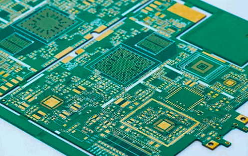
When it comes to printed circuit boards, there are a variety you can choose from to cater for the needs of your product, from single-sided boards to multi-layer or even flexible boards. Each of these circuit boards has a different number of layers that contribute to their functionality, making them the right choice for different tasks.
1. TOP Layer: The top copper foil trace,if it is a single panel, there is no such layer.
2. Bottom Layer: The bottom copper foil trace.
3. Top/Bottom Solder Layer: The top layer/bottom layer is laid with solder mask green oil to prevent tin on the copper foil and maintain insulation. Open windows with solder mask green oil at pads, vias and non-electrical traces on this layer.
4. Top/Bottom Paste Layer: This layer is generally used during the SMT process.
5. Top/Bottom Silkscreen Layer: Designed as a variety of silkscreen logos, such as component tag numbers, characters, trademarks, etc.

6. Mechanical Layer: Designed as a PCB mechanical shape, the layer 1 is the outline layer. Other layer 2/3/4 can be used as mechanical dimension marking or special purpose. For example, when some boards need to make conductive carbon oil, layer 2/3/4 can be used, but the purpose of this layer must be clearly marked on the same layer.
7. Keepout Layer: It is designed as a prohibited wiring layer. Many designers also use it as the mechanical shape of the PCB. If there are keepout and mechanical layer 1 on the PCB at the same time, it mainly depends on the shape integrity of these two layers. Generally, mechanical layer 1 shall prevail. It is recommended to use mechanical layer 1 as the shape layer as much as possible when designing. If you use keepout layer as the shape, do not use mechanical layer 1 to avoid confusion!
8. Midlayers: Mostly used for multi-layer boards. It can also be used as a special-purpose layer, but the purpose of this layer must be clearly identified on the same layer.
9. Internal Electrical Layer: Used for multi-layer boards.
10. Through-hole Layer: Through-hole pad layer.
11. Drilling Positioning Layer: The center positioning coordinate of the vias hole and the pads.
12. Drilling Description Layer: The drilling hole size description of pads and vias.
Victory is a professional PCB manufacturer which established in 2005. Adhere to be a specialized manufacturer for multiply species, small to medium series, and quick turn production, we insist to provide 3H(high quality, high precision and high density) PCBs for our customers. If you have any inquiry, please do not hesitate to contact us.