WHAT IS THE PCB MANUFACTURING PROCESS?
The printed circuit board (PCB) manufacturing process requires a complex procedure to ensure the performance of the finished product. Though circuit boards can be single, double or multilayered, the fabrication processes used only differ after the first layer’s production. Due to differences in the structure of the PCBs, some may require 20 or more steps during manufacturing.
The number of steps required for producing printed circuit boards correlates to their complexity. Skipping any step or cutting back on the procedure could negatively impact the performance of the circuit board. However, when successfully completed, the PCBs should perform their tasks properly as key electronic components.
WHAT ARE THE PARTS OF A PCB?
There are four main parts to a PCB:
Substrate: The first, and most important, is the substrate, usually made of fiberglass. Fiberglass is used because it provides a core strength to the PCB and helps resist breakage. Think of the substrate as the PCB’s “skeleton”.
Copper Layer: Depending on the board type, this layer can either be copper foil or a full-on copper coating. Regardless of which approach is used, the point of the copper is still the same — to carry electrical signals to and from the PCB, much like your nervous system carries signals between your brain and your muscles.
Solder Mask: The third piece of the PCB is the solder mask, which is a layer of polymer that helps protect the copper so that it doesn’t short-circuit from coming into contact with the environment. In this way, the solder mask acts as the PCB’s “skin”.
Silkscreen: The final part of the circuit board is the silkscreen. The silkscreen is usually on the component side of the board used to show part numbers, logos, symbols switch settings, component reference and test points. The silkscreen can also be known as legend or nomenclature.

HOW IS A PCB MANUFACTURED?
The steps of the PCB design process start with design and verification and continue through the fabrication of the circuit boards. Many steps require computer guidance and machine-driven tools to ensure accuracy and prevent short circuits or incomplete circuits. The completed boards must undergo strict testing before they are packaged and delivered to customers.
Step One: Designing the PCB
Step Two: Design Review and Engineering Questions
Step Three: Printing the PCB Design
Step Four: Printing the Copper for the Interior Layers
Step Five: Etch the Inner Layers or Core to Remove Copper
Step Six: Layer Alignment
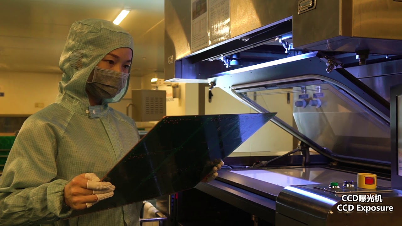
Step Seven: Automated Optical Inspection
Step Eight: Laminating the PCB Layers
Steps Nine: Drilling
Steps Ten: PCB Plating
Step Eleven: Outer Layer Imaging
Step Twelve: Outer Layer Etching
Steps Thirteen: Outer Layer AOI
Steps Fourteen: Solder Mask Application
Step Fifteen: Silkscreen Application
Step Sixteen: Finishing the PCB
Step Seventeen: Electrical Reliability Test
Step Eighteen: Profiling and Route Out
Step Nineteen: Quality Check and Visual Inspection
Step Twenty: Packaging and Delivery
Heavy Copper PCB Application
Thick copper circuit board is mainly used
In the field of transportation (such as automotive electronics, rail traffic signal control),
medical instruments,
Aerospace industry and industrial control and other fields.
CONTACT VICTORY PCB FOR QUESTIONS
High-quality engineering and manufacturing of PCBs are critical components of the operations of the circuit boards in electronics. Understanding the complexities of the process and why each step must occur gives you a better appreciation for the cost and effort put into each printed circuit board.
When your company needs PCBs for any job, contact us at Victory PCB. We work to supply small and large batches of competitively priced printed circuit boards to our customers.


