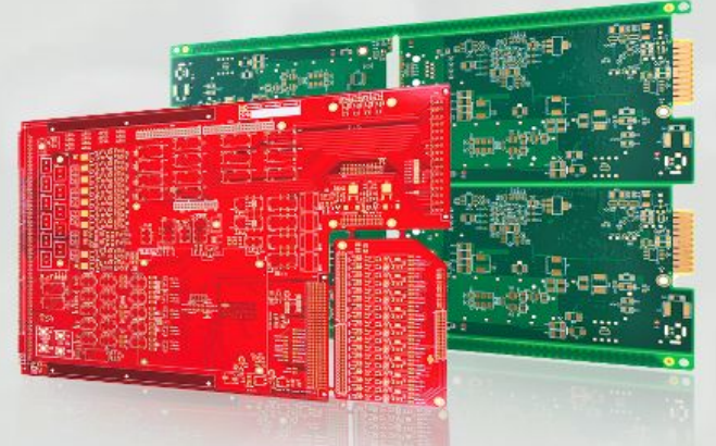
Have you ever considered what footprint in PCB design does? You need to understand what Printed Circuit Board (PCB) design is, first. PCB is a non-conductive copper sheet coated with a polymer material used to connect and support electronic components joined together through a conductive pathway or etched.
PCBs provide mechanical support as well as electrical support to integrated circuits and other components that are common in most electronic devices. For example, a computer motherboard, radio or television panel, rechargeable torch pads, phone panel, headset pads, and so on. All these gadgets cannot function without PCB manufacturers producing quality circuit boards that fit neatly.
Therefore, a footprint in PCB is a design or sketch that shows how electronics components or integrated circuits (ICs) will be joined together by soldering. So, if it is a large ball grid (BGA) or a through-hole connector, or a surface mount capacitor, every unit needs to follow a footprint for them to be soldered into a printed circuit board.
Sometimes, the footprint and its arrangement of metal pads are what the integrated circuits (ICs) will be soldered onto and it is called a landing pattern. Therefore, a footprint should be designed in such a way that it is easy to use and that exacts standard for the right assembling of the PCB.

When ICs or pads are in the wrong location, the possibility of wrong soldering is high. When the footprint design is faulty, you are likely to assemble units too close to each other. Hence, to assemble the best footprint for your next PCB design note the following guidelines.
You would likely encounter complications if you did not consider PCB footprint creation guidelines. When printed circuit board design was first introduced into the market, proper attention was not given to the creation of PCB library parts and PCB manufacturers were able to get away with following the footprint guidelines strictly.
For example, through-hole connector bypass footprint caps, most often than not, are generically created with 0.30 inches pin spacing as well as approximately 0.50 inches of drawn outline in all directions of the pins in the absence of perusing the datasheet for the particular electronic component under usage.
Also, single inline parts (SIP) and dual inline parts (DIP) that are through-hole footprints including their connectors as well as headers are also manufactured in likewise manner. It is surprising to imagine that the design space is giving up because the footprints are unnecessarily huge.
Furthermore, the capacitors bypass might end up being designed twice the original size. This gives room for large unused space around the capacitors. This unused space becomes obvious when especially, several of it is lined up in a row visible on the board.
Another problem is wrong pad sizes – a large pad will cause surface mount technology fragments to drift out of position or take up space for trace routing when soldered. A small pad will result in breakout challenges for through-hole fragments as well as poor solder linkage for surface mount technology (SMT).
Nowadays, PCB manufacturers are aware of the importance of following PCB footprint creation guidelines and the comfort it brings to their customers. And not only that, we are ready to serve you the best. Click here to contact us, today.