PCB panelization is a crucial process in electronics manufacturing. By grouping multiple individual PCBs onto a single larger board, manufacturers can streamline production, reduce costs, and enhance efficiency. This guide explores the benefits, methods, design considerations, and best practices for effective PCB panelization.
PCB panelization is the process of combining several individual printed circuit boards (PCBs) into a single larger board, known as a panel, during manufacturing. This technique allows for multiple boards to be processed simultaneously, significantly improving throughput and simplifying handling during assembly. Historically, PCB panelization evolved as manufacturers sought ways to increase production efficiency and reduce costs. Today, it is a standard practice in the electronics industry, underpinning the mass production of everything from consumer electronics to advanced industrial equipment.
Panelization allows multiple boards to be processed at once, saving time and reducing handling efforts. This bulk processing capability is particularly beneficial in large-scale production runs, where time and labor savings can be substantial.
PCB panelization can improve the utilization rate of the board, thereby reducing production costs. Since the products of each industry are different, the size of the applied pcb circuit boards is also different. Some of the PCB circuit boards in the electronics industry are relatively small, and are often designed in a way of imposition, which not only facilitates the processing and production of electronic factories, but also It can also reduce the waste of the board and reduce the cost.
Panels are easier to handle and transport compared to individual PCBs, reducing the risk of damage during these processes. This enhanced durability is crucial in maintaining the integrity of the boards throughout the manufacturing cycle.
The ability to assemble components on multiple boards simultaneously makes the process more efficient. This simultaneous assembly not only speeds up production but also ensures consistency and uniformity across all boards in a panel.
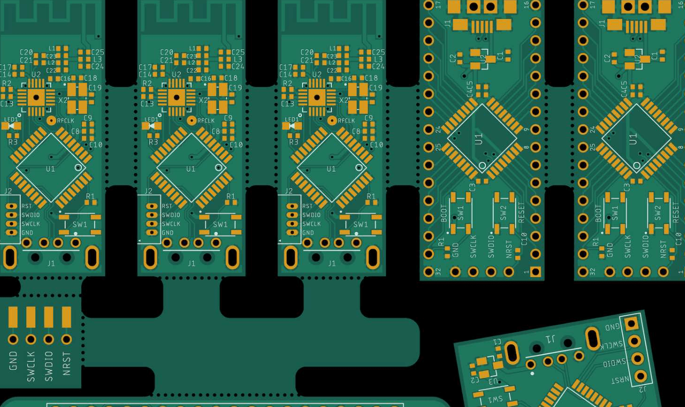
V-Scoring involves cutting shallow V-shaped grooves along the edges of each PCB within the panel. This technique allows the boards to be easily snapped apart after assembly. Advantages of V-Scoring include simplicity and cost-effectiveness, while disadvantages may include limited design flexibility and potential stress on the boards during separation.
Tab Routing uses tabs with or without perforations to hold individual PCBs together. After assembly, the tabs are broken or cut to separate the boards. This method offers greater design flexibility and strength, making it suitable for complex or delicate PCBs. However, it can be more time-consuming and may leave rough edges that require additional finishing.
For complex designs, a combination of V-Scoring and Tab Routing can optimize the panelization process. This hybrid approach leverages the strengths of both methods, providing a balance of flexibility, strength, and ease of separation.
Here’s a table that compares V-Scoring and Tab Routing methods for PCB panelization:
| Parameter | V-Scoring | Tab Routing |
|---|---|---|
| Board Separation | Boards are snapped apart along the V-grooves. | Tabs are broken or cut to separate the boards. |
| Design Flexibility | Limited to straight lines; best for square or rectangular shapes. | Greater flexibility; suitable for complex or irregular shapes. |
| Edge Quality | May require additional sanding due to rough edges. | Generally results in smoother edges; may have minor nubs. |
| Manufacturing Time | Faster, as machines can quickly cut V-grooves. | Slower, as it involves more intricate routing processes. |
| Cost | Generally lower due to simpler process. | Higher due to increased complexity and additional steps. |
| Component Clearance | Requires components to be kept 0.05 inches from the edge. | Components should be at least 0.125 inches from tabs. |
| Material Waste | Less waste compared to tab routing. | More waste due to the routing process. |
| Panel Strength | Lower, as V-grooves reduce the overall strength. | Higher, as tabs provide more structural integrity. |
| Handling Stress | Potential for stress fractures at the V-grooves. | Less stress on the board during separation. |
| Suitable For | Standard, high-volume production of rectangular boards. | Complex designs, low to medium volume production, or boards with edge components. |
While V-Scoring and Tab Routing are the most common panelization design methods, several advanced techniques are used for separating boards, each suited for specific requirements and volume considerations.
Laser Depaneling: This is a high-precision, non-contact method that uses a focused laser beam to ablate the board material along the cut line. It is ideal for the most delicate boards and sensitive components, as it generates zero mechanical stress, produces a clean edge, and can handle extremely complex, non-linear shapes. However, it is typically the highest-cost option.
Router Depaneling: This method uses a high-speed rotary routing bit to mill through the tabs and perimeter of a panel. It is highly effective for separating panels with complex or irregular outlines that were created using tab-routing. It offers a good balance of precision and speed but generates dust and requires proper dust extraction systems.
Punch Depaneling: Best suited for very high-volume production of simple, fixed shapes. A custom die (like a cookie cutter) is created to punch out individual boards from the panel in a single action. This is an extremely fast method but lacks flexibility, as a new, costly die must be manufactured for every unique board shape.
Tab routing panelization tends to be preferred in applications where components are placed very close to or over an edge. It’s also preferable for PCBs made in non-rectangular shapes like circles. However, because the tabs are the breaking points for these arrays, several design choices must be made to ensure the strength and functionality of these arrays, especially during the breakout process. Some of these considerations include:
Clearance: Because of the stress placed at the breakaway points and the potential for splintering, keep components and traces at least 1/8 inches away from the tabs. Surface-mounted multilayer ceramic chip capacitors must be kept further away, at least ¼ inches from the tabs to ensure minimal interference.
Knock-Outs: If your PCB design includes holes greater than 0.6 inches, a placeholder, or knockout, may be required to prevent issues during the wave-solder process. Knockouts are particularly important in the middle of an array, where PCB arrays are more likely to sag. Smaller rectangular knockouts can have a wide, five-hole perforated tab on a single edge, while larger, more irregular shaped knockouts may require multiple three-hole perforated tabs.
Tab Placement:Tab placement is important to maintain the integrity of your PCB array design. Tabs must be placed every 2 to 3 inches along a board edge for five-hole perforated tabs, and every 1.5 inches for three-hole perforated tabs. Tabs should be placed as close to the edge of a board as possible to avoid curving at the edge of a board, but should not be placed under overhanging components. The designer must also ensure the tabs are big enough to support the boards, but not big enough to interfere with the breakout process.
Perforation Placement: If you want to avoid protrusions from the side of your board, never place tab perforations down the center of a tab – instead, run them close to the edge of the PCB, or on each side of the tab if placed between two PCBs.
Array Arrangement:When arranging PCBs, be sure all tabs broken at one time are collinear so that there are consistent break-lines throughout the array. If break-lines aren’t consistent, some tabs will break while others are simply pulled perpendicularly to the board surface, which can tear the lamination.
Victory is a professional PCB manufacturer which established in 2005. Adhere to be a specialized manufacturer for multiply species, small to medium series, and quick turn production, we insist to provide 3H(high quality, high precision and high density) PCBs for our customers.
With a total plant area 30,000sq.m, our monthly capability can be 60,000sq.m with 3000 parts. With advanced PCB production and testing equipments, and well-found quality system to monitor throughout the whole manufacturing to assembly, we can ensure the stable and excellent quality of the production process to meet customers’ requirements. If you are looking for a reliable and professional supplier of PCB, please contact us for more information.
1. What are the standard PCB panel sizes?
Most manufacturers use 18″ x 24″ or 18″ x 12″ panels, which optimize manufacturing efficiency. The ideal size depends on your board dimensions and the fabricator’s equipment.
2. How does panelization affect cost?
While adding a step, panelization reduces overall cost by improving material yield and assembly throughput. V-Scoring is more economical than Tab Routing for suitable designs.
3. Can flexible PCBs be panelized?
Yes, flex circuits are typically mounted on rigid carrier panels using temporary adhesives. Laser cutting is recommended for stress-free separation of the flexible boards.
4. What are tooling holes and fiducial marks, and why are they important in a panel?
Tooling holes are precision holes in the panel rails used to mechanically align and secure the panel during manufacturing. Fiducial marks are small copper dots that serve as optical reference points for automated assembly equipment. Both are critical for ensuring accurate component placement and consistent registration across all production steps.


