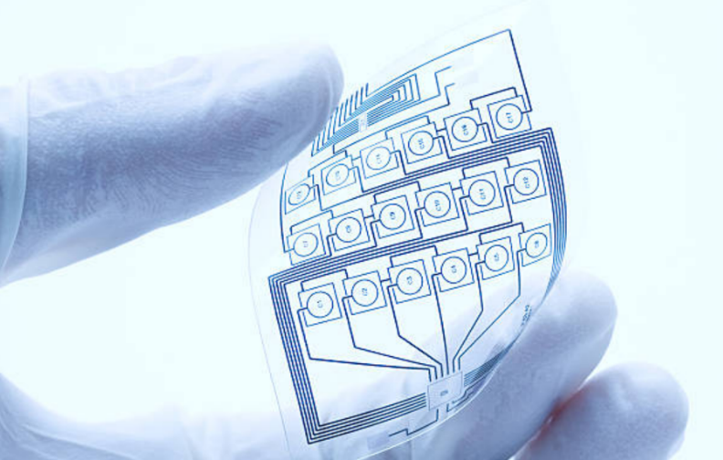
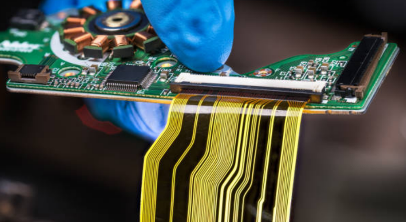
A flexible PCB substrate is also called FPC (Flexible printed circuits). The greatest feature of this substrate is its thinness and softness. Its electrical characteristics do not change even if it is bent, which has the advantage of demonstrating its performance. It has a structure in which a base film (such as polyimide), which is a thin-film insulator, is used, and an adhesive layer and conductor foil are laminated on it.
Flexible PCB substrates are characterized by their shape and usage. It can be bent due to its greatest characteristics of "thinness" and "softness", so it can be said that it is a substrate with a high degree of freedom. Moreover, since the electrical characteristics do not change even when bent, it has the advantage of maximizing its characteristics.
Utilizing this feature, it is used as a connection cable that connects movable parts, bent parts, substrates that are required to be thinner and lighter, and units. Examples of familiar uses include keyboards, calculators, LCD monitors, and printer heads.
In addition, it is almost always used in movable parts such as foldable mobile phones and three-dimensional circuits such as camera lenses. This substrate is widely used in space development and aviation, where weight reduction is particularly important.
It is mainly used in places where there is a lot of movement. As a feature, it specializes in thinness, flexibility, and light weight, and it is possible to use the substrate even in a narrow place where it is difficult to realize. Of course, it is highly durable and can be used without problems even when it is folded or moved many times.
It is used when you want to increase functionality. The feature is that it is also suitable for high density, and it can increase the degree of design freedom and functional improvement when you want to create more complicated circuits such as cross wiring. On the other hand, unlike the single-sided structure, the movable durability is reduced.

In addition to single-sided and double-sided structures, there are multilayer structures and rigid/flex structures.
Flexible PCB substrates and rigid substrates have similar basic processing processes, chemically etching the copper foil of copper-clad laminates to form circuits. Through-hole structures are made in the same way. The major difference in terms of composition and processing is protection of the circuit surface. In general, rigid boards are printed with a solder mask, while flexible boards are laminated with a plastic film called coverlay.
Next, if you think about the usage, both can be considered completely different things. This is because the main purpose of a rigid board is to mount and wire various electronic components, while the main purpose of a flexible board is to use it as a cable. Below is a comparison table of both boards.
The adhesive type was first put to practical use as a copper-clad laminate for flexible PCB substrates. This type of manufacturing process begins by applying an adhesive to a base film, allowing it to dry, then overlaying a copper foil on top and applying heat and pressure to finish.
The adhesive type has the longest track record and is also widely used today because of its low price.. Adhesive-type copper-clad laminates are generally manufactured in roll form, but some manufacturers manufacture them in sheet form in order to meet the demand for high-mix, low-volume production.

Thermosetting resins such as epoxy resins and acrylic resins are used as adhesives for copper-clad laminates. The performance of these adhesives varies greatly depending on their composition and bonding conditions. There are many differences between manufacturers.
Thermosetting resins generally have high heat resistance, but they are still inferior to polyimide resins. Therefore, the heat resistance of adhesive-type copper-clad laminates is determined by the adhesive.
Adhesive-type copper-clad laminates offer a wider choice of materials. In addition to standard polyimide film, PET film, PEN film, etc. can be used as the base material. Materials such as thin glass epoxy sheets and paper can also be used. On the other hand, conductors can be made from special metal foils such as aluminum foil and stainless steel, in addition to standard electrolytic copper foil and rolled copper foil.
In adhesive-type copper-clad laminates, electrical properties such as insulation, mechanical properties such as adhesive strength and flex resistance, and chemical properties such as flame retardancy and chemical resistance vary greatly depending on the bonding conditions with the adhesive increase.
Its adhesive resin is prepared by the copper clad laminate manufacturer. Therefore, even if the base film and copper foil are the same, the adhesives and process conditions of the copper-clad laminate manufacturer will make a big difference.
In adhesive-type copper-clad laminates, the thickness of the adhesive layer is the same as that of the base film, so it cannot be ignored when considering the thinness and flexibility of flexible PCB substrates. As a result, various ideas were devised for constructing copper-clad laminates without using adhesives.
The casting type was the first practical copper-clad laminate that does not use an adhesive. Because it is thin and has good heat resistance, it has come to be used as a standard for multilayer circuits and high-density circuits.
Although the structure looks simple, the manufacturing method is not simple.
In the casting method, a liquid polyimide resin material is evenly applied directly onto the prepared copper foil, and a high-temperature heat treatment (300°C or higher) is applied to form a film, and the copper-clad laminate is completed at once. Unfortunately, polyimide resin, which can be used as a base film, does not adhere to metal.
Therefore, a thin coating of a polyimide resin agent, which has adhesiveness with metal and high affinity with the core polyimide resin, is applied as a base. However, since the balance as a film is not good with only one side, the other side is also coated. In other words, the base polyimide film has a three-layer structure.
A double-sided copper-clad laminate cannot be directly produced by the casting method. Therefore, a double-sided copper clad laminate must use a thermoplastic (melting at elevated temperature) polyimide resin as the underlying polyimide adhesive layer, and finally laminate a second copper foil. Lamination temperatures are usually quite high, above 300°C.
In addition to standard electrolytic copper foil and rolled copper foil, alloy foil such as stainless steel can also be used for conductors. There are no thickness restrictions. In the case of both sides, it is also possible to combine conductor foils of different materials and thicknesses. However, since it is usually manufactured by a roll-to-roll process, it is not so good to deal with a wide variety of products.
There is generally only one type of base film composition for each manufacturer. Due to the manufacturing process, the thickness range is limited to 12.5-50 µm.
The sputtering/plating type can easily produce the thin conductor foil copper-clad laminates required for fine circuit formation. Therefore, flexible PCB substrates used as substrates for display driver circuits are used in fine circuits with a pattern pitch of less than 50 μm, such as TAB circuits (Tape Automated Bonding) and COF circuits (Chip on Film).
The starting point of the manufacturing process is the base film.
In this type of copper-clad laminate, the conductor layer is formed on the base film by electroplating, but electroplating cannot be applied directly to the insulating base (plastic) film.
First, a thin conductive layer is formed on the surface of the film using a metal such as nickel or an alloy using a vacuum sputtering method. This is called a seed layer. The thickness is usually less than 0.1 μm. Once the seed layer is in place, metal can be electroplated onto it to any desired thickness.
The seed layer must have stable adhesion to the base film. In general, the roll-to-roll vacuum sputtering process is not very flexible, so it is not suitable for high-mix low-volume production.
Since this method does not require a high-temperature process, it is technically possible to use PET film or PEN film with low heat resistance as the base material. However, most of the products on the market are copper-clad laminates based on polyimide film.
Also, there should be no technical limit to the thickness of the base film, but what is actually on the market is a copper-clad laminate that uses a film with a thickness of 12.5 to 50 μm.
In addition, since the conductor layer is formed by electroplating in this method, the degree of freedom in conductor thickness is large, but the thicker the conductor, the higher the manufacturing cost. Conversely, it is easy to make a thin conductor layer.
However, from a cost perspective, what is actually on the market is a thin copper-clad laminate with a conductor thickness of less than 10 µm, and conductors with a thickness of less than 1 µm are also possible. In order to form fine circuits with a pattern width of less than 30 μm by etching, a copper-clad laminate with such a thin conductor foil is required.