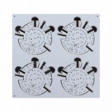
The advent of double-sided PCB has gradually filled up the void created by the growing demand for the processing of sophisticated electronics.

It's high-level performance and effectiveness has made open doors for the innovative application of electronics.
The huge merits of double-sided printed Circuit Boards have made it the main PCB used by most businesses all over the world.
That’s not all; you also get to enjoy customized Double-Sided PCB produced to particularly meet your needs.
These Customized PCBs enable you to develop and also design Printed Circuit Boards based on your product description.
With this, it helps in giving the quality and performance of your product an incredible boost.
To this end, it is very imperative to have a good background understanding of the production processes of the double-sided PCBs.
Obviously, this will really help in choosing the most suitable Printed Circuit Board for your products.
Well, for the best performance, sourcing your double-sided PCBs from a trusted manufacturer is the best way to have the best deal.
However, if for any reason you are not conversant with the procedures for the manufacture double-sided PCB, the do not despair, because we have you covered.
Below is a short but powerful guide on the double-sided Printed Circuit Board manufacturing process
1.Preparation
The first step is to prepare the material you intend to use. This involves drilling the entry materials as well as the copper-clad panels and ensuring that they are kept close.
You should remember that every standard panel usually has a solid base material of about 1.6mm. Its covering consists of 18 µm of copper on each side.
2.Pinning
After making all the necessary holes on the tolling tools, the next thing to do according to the manufacturing process is to ensure that the PCB panel is not pinned on the CNC machine.
3.Printed Circuit Board CNC Drilling
Regarding this step, the general drilling technique used is the Through-hol technique. However, other techniques can be chosen to achieve the same goal.
Also, the drilling technique used in the production of double-sided PCB is quite different from that used for the production of single-sided PCB.
After this, component drills are created and the through-holes plated through the aid of a CNC drill device.
4.Through-hole plating
Here, electrographic films, mostly Palladium are used to electroplate the wall structures of the drilled cavity.
This step makes the galvanization of copper which is one of the most important last stages of the production process very possible.
Apart from Palladium, which is most preferred and common, any other electrographic film can be used for this process.
5.Brushing
Since it is very important for Printed Circuit Board to be completely free from any form of dirt, it must be carefully cleaned before the next stage.
To achieve this, the most suitable method is known as Brushing. This is quite compatible with the production processes of the double-sided PCB.
6.Laminating
The production stages of PCBs will remain incomplete with the lamination of the PCB panels. This can only be achieved when a very high temperature and pressure are present.
7.Avoid Exposure
After lamination ensure the panels are not exposed to UV-lights by using photo plots that are highly resistant to this kind of light.
8.Development
When the PCB creates about 1% of the sodium carbonate via the cycling building, it means that the PCB is actually ready for the plating.
Through the process of cycling Building, PCBs produce about a percent of sodium carbonate, do watch for this. Once this is observed, you should prepare the PCB for plating.
9.Electroplated Configuration
This is the earliest stage of the plating process; you ensure that the pads and tracks are on the board and then copper plated.
Note that their thickness is around 35 µm, therefore to join it will require a thin film that ranges from 6 µm to 10 µm.
The fusing is very necessary as it ensures that the tracks and pads are protected when undergoing the final etching process.
10.Avoid Stripping
This can be achieved using 2.5% of caustic potash which allows the panel to a photoresist
11.Etching
This involves spraying ammonia on the copper film. The reason for this is to eliminate any form of unwanted copper.
12.Tin Stripping
The elimination of tin is achieved using nitric acid. The tin – stripping stage is followed by the spraying and dipping stages.
13.Solder mask Applications
The preliminary stage of spraying and screen- printing is to apply the solder mask.
14.Exposure
Finally, after spraying, the solder mask is exposed to sunlight, and since double-sided PCB is being manufactured, photo plots are the most suitable to use.
Thereafter, the silkscreen is engraved on the solder mask providing the basic landing for the surface finish. The surface finish comprises nickel and gold, it is used in vertical baths.
In order to enhance its ability to be soldered gold plating on the nickel surface during the manufacturing process should not be undermined.
Wrap Up
There you have it all. All the steps involved in the production of double-sided printed circuit boards.
For the best value and experience for all your double-sided PCB needs, always consider sourcing them from a professional manufacturer.