Modern electronics use Ball Grid Array technology (BGA) for its high efficiency and performance. This post discusses the differences between SMD and NSMD pads in BGA designs that are important to optimize PCB functionality.
Here’s a table summarizing the key differences between Solder Mask Defined (SMD) and Non-Solder Mask Defined (NSMD) pad types:
| Feature | SMD Pad Type | NSMD Pad Type |
|---|---|---|
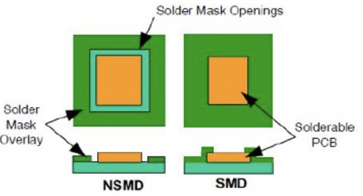
| Solder Mask Opening vs. Pad | The solder mask opening is smaller than the metal pad. | The solder mask opening is larger than the metal pad. |
| Pad Coverage | Solder mask overlaps the edges of the metal pad. | Solder mask does not overlap the pad; the entire pad is exposed. |
| Advantages | Minimizes underfill issues Prevents solder spillage |
Enhances board-level mechanical performance Stronger solder bond due to solder flow |
| Application | Preferred for precision and minimal underfill issues in surface mount assembly | Preferred for applications requiring enhanced mechanical strength and thermal reliability |
| Solder Joint Characteristics | More precise solder joints with reduced risk of solder bridging | Stronger mechanical bond due to increased solder flow around the pad |
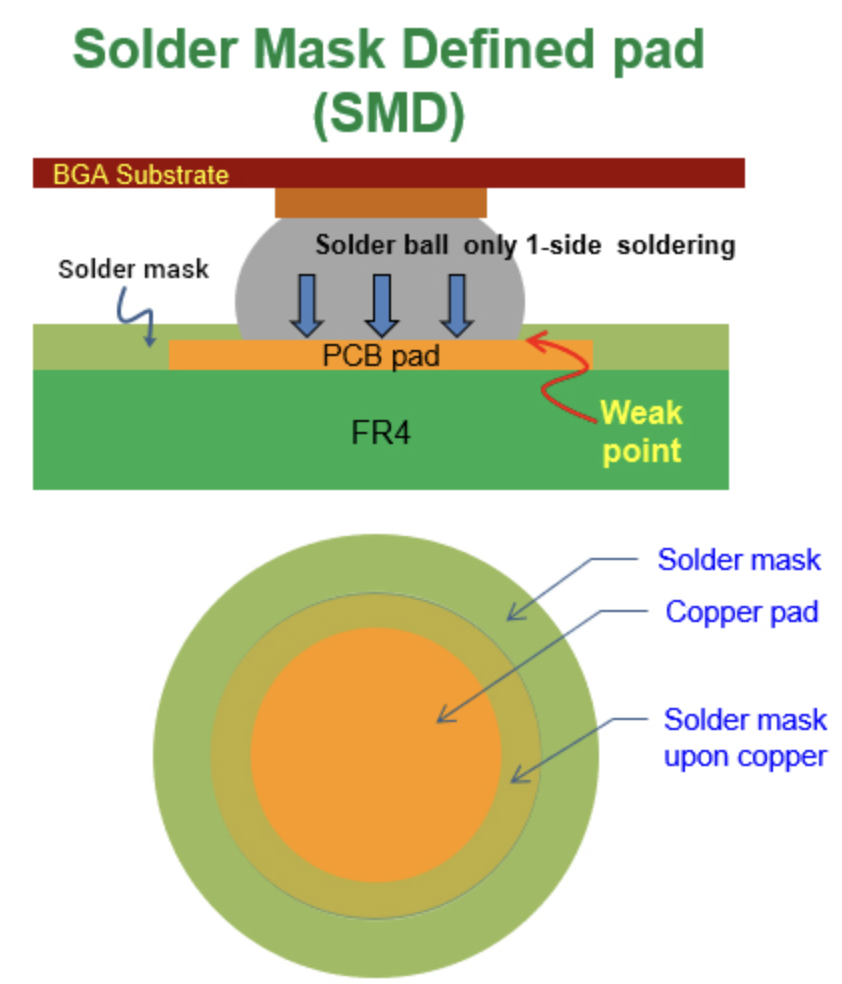
Solder Mask Defined, has a bigger copper pad size than the solder mask open area. That means the solder mask covers the copper pad, and its open dimension will define the soldering pad size.
SMD pads design has better copper pad bonding strength on PCB. It also improves the BGA bonding strength because the copper pad size of SMD is bigger than that of NSMD. The larger the copper size, the greater the PCB bonding strength.
SMD pads design has better performance to survive from the impact drop test. According to the data provided by the PCB supplier, there is a 53% improvement in the pad bonded on PCB strength compared to the NSMD pad designs.
Lower Soldering Strength: The SMD pads design will lower the soldering strength because the solder mask will expand its dimension and reduce the soldering size during the high-temperature reflow stage.
Poor Tolerance Control: The solder mask printing will shift due to poor tolerance control. This will cause a position discrepancy between the BGA ball and pad on the PCB. Some serious cases will affect the solder pad dimension on the PCB.
Trace Layout Difficulties: The trace layout is more difficult between pads for SMD pad design because the bigger pad size makes the small space between pads.
NSMD, or Non-Solder Mask Defined, also called Copper Defined Pad Design, features a copper pad smaller than the solder mask hole. The design exposes the entire copper pad by not covering it, leaving a gap. This approach, contrasting with SMD, bases the pad size on the copper itself, not the mask, offering a distinct advantage in soldering accuracy and connection strength.
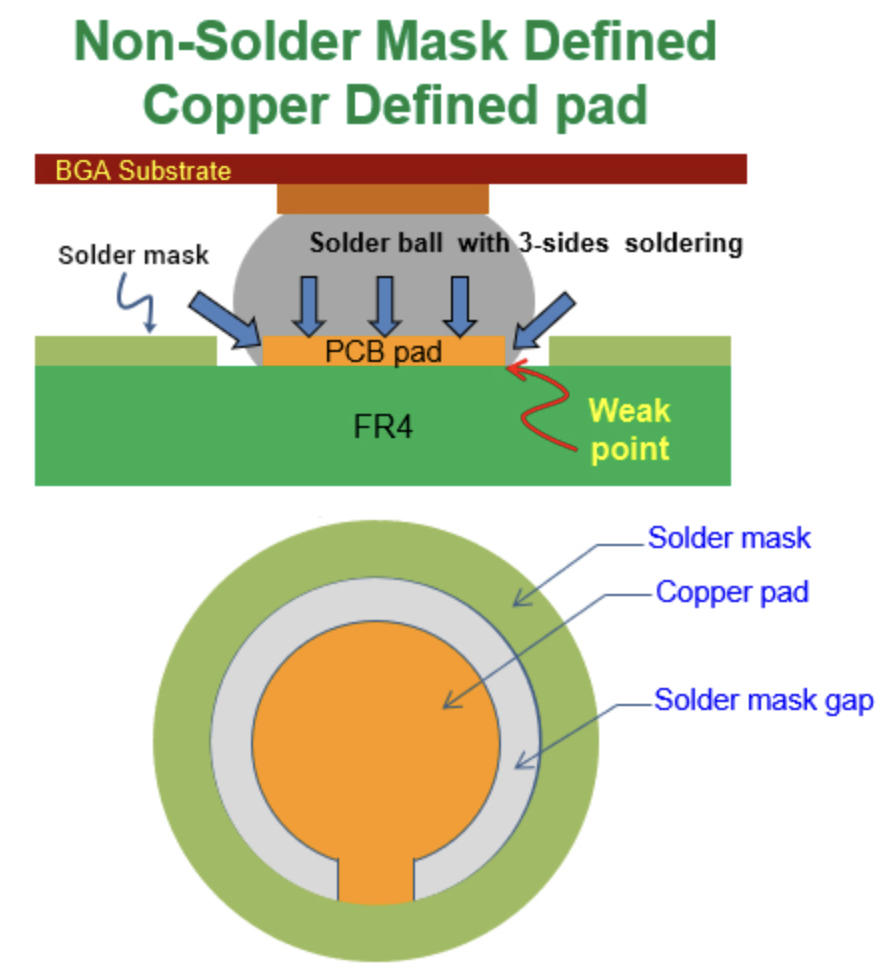
Good solderability: The soldering area is not only the copper pad surface but also the surrounding side of the copper pad.
Precise Pad Size and Location Control: PCB suppliers will easily control the soldering pad size and the location of the NSMD. Because the copper pad is registered by optical exposure skill, and it is more accurate technology.
Improved Trace Layout Flexibility: NSMD (Non-Solder Mask Defined) pad designs can make trace layout easier than SMD (Solder Mask Defined) pads due to the smaller size of the copper pads in NSMD designs.
Reduced Mechanical Strength: The smaller size of NSMD pads can reduce solder attachment area, potentially lowering the mechanical bond strength of components on the PCB—for example, a BGA ball cracks during the impact drop test.
Problems with underfill glue: Many companies apply underfill glue to enhance the strength of their BGA bonding. The underfill process increases manufacturing costs and wastes material and labor. The underfill makes the repair difficult since the glue is fixed under the BGA.
Choosing between SMD and NSMD pads for BGA packages in PCB design involves assessing several factors to meet specific design requirements, enhance performance, and ensure reliability. Here’s a focused guide to help in making this decision:
For flex boards, which are prone to bending and flexing, and small devices (smaller than 0402), using SMD (Solder Mask Defined) pad designs is beneficial. The solder mask helps define the pad boundaries, providing additional mechanical strength to the solder joints, which is crucial for the durability of flex boards and the reliability of connections on small components.
NSMD (Non-Solder Mask Defined) pads are preferred for larger components due to their simpler design and the larger copper area exposed for soldering. This larger area can enhance the electrical connection and heat dissipation, which are important factors for the performance of larger components.
A mixed approach can be effective in BGA designs. Functional pins, which require robust electrical connections and potentially benefit from the added mechanical strength, can use SMD designs. Fixed pins, which may not require the same level of electrical performance and benefit from easier soldering and better heat dissipation, can utilize NSMD designs. This mixed strategy leverages the strengths of both pad types to optimize the performance and reliability of BGA components in the circuit.
| Criteria | SMD Footprints Preferred | NSMD Footprints Suit |
|---|---|---|
| BGA Package Pitch | Fine pitch BGA packages ≤ 0.8mm Small BGAs with pitch ≤ 0.5mm |
Lower density BGA packages with >1mm pitch |
| Package Size | Packages with high pin counts | Larger package sizes above 15mm x 15mm |
| Application Space Constraints | Portable consumer electronics where space is critical | – |
| Process Tolerances | – | Automotive grade parts needing greater process tolerances |
| Soldering Requirements | – | Corner ball cases requiring dogbone pads for sufficient solder volume |
| PCB Design Complexity | – | Boards with fewer routing layers where pad spacing is less critical |
| Solder Voiding Risks | – | Applications where solder voiding risks need minimization |
Understanding the differences between SMD and NSMD pads is crucial for BGA design, affecting reliability and performance. Choosing the right pad type ensures optimal PCB functionality. For expert PCB design support, contact VictoryPCB via [email protected], we’ll be glad to help you.


