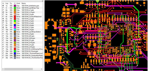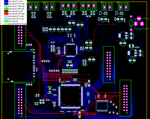
To produce a tile in a professional plant, commonly known as a tile shop, we need to prepare Gerber files. This is a certain standard, thanks to which the tile shop does not have to have all possible design programs, such as Kicad, Eagle, Protel, and Altium which would be incredibly expensive.
Each program generates a mosaic of paths in the universal Gerber format to simplify and standardize the production process.
Each Gerber file contains a separate layer; the distinguishing feature is the file extension. It is even crucial because, after the extension, the producer can recognize what layer he is dealing with.
Let's see the cross-section of the printed circuit board. It has a visible layered structure.
· Glass-epoxy laminate - stiffens the entire structure and is a good insulator.
· Copper layer - a copper foil is applied to the laminate, from which paths, mass fields, etc., are etched.
· Solder mask - usually green and used to protect copper against short circuits and oxidation. It is something like varnish or thin foil in which holes are made for soldering pads.
· The descriptive layer includes labels, element numbers, values, comments, and other graphic elements; this is an optional layer that can be there if we want to cut costs.
If the board is double-sided, then the layers of copper, solder mask, and descriptions are also on both sides.

A characteristic element of a double-sided board is a grommet, which connects tracks on opposite sides. It is an ordinary drilled hole that has a metallization inside. The vias can be covered with a solder mask or be beige uncovered.
If uncovered, they can be used as test points, and you can temporarily solder something to them. Regular solder pads for through-hole components also have metallization and can be used as vias. The metalized hole cannot be reamed to increase its diameter!
So if you need to figure out which diameter is right, it's better to have it too big or too small!
The procedure for ordering a board is as follows.
1. design the board
2. Generate Gerber files (files required for board manufacturing)
3. Request a company's manufacturing service (file upload -> payment)
A Gerber file records information such as the board outline, wiring, and the pad positions of parts, which are necessary for the board manufacturing company to manufacture the board.
This data is submitted to the board manufacturing company when placing an order.
The Gerber files are the files that the designer sends to the PCB manufacturing company for the industrialization of the boards.

It is uncommon for the designer to send the complete PCB design to the manufacturer. Instead, the Gerber files are sent, which contain all the information the manufacturer needs – and nothing more. Gerber files contain no information about the components used or other details on the circuit schematic.
Now that we consider that our PCB project is finished, we can start the process of generating the gerbers. It is essential to remember that after generating the gerbers, we must keep the schematic and the layout the same. If it is unavoidable to make changes, the Gerber generation process must start from scratch.
We will start by opening the "amplification. brd" file and clicking on "File > Run ULP…". A window will appear where we must select the "drillcfg.ulp" file. After that, another window will appear where we must choose the "mm" option.
EAGLE will then show a window listing all the hole diameters on the board. It is inconvenient to edit this list, and we must click "Ok."
The result will be a file with a ".drl" extension that should be saved together with the other project files. This file contains information about the diameter of the holes in the plate and will be used in future steps.
After saving the ".drl" file, the next step is, in the ".brd" file window, clicking on "File > CAM Processor…". A new window will appear. This is the "CAM Processor," the EAGLE Gerber generation tool. Through the "CAM Processor," it is possible to generate Gerber files in different formats and follow the designs' exact configurations.
In the "CAM Processor," it is possible to manually configure all the parameters of the Gerber files we want to generate. Still, to our delight, EAGLE already offers some ready-made routines for generating Gerber files that already serve most cases.
Most PCI manufacturing companies use the RS274X format, and a routine is ready to generate this Gerber file format. To use it, in the top menu of the "CAM Processor" window, we must click on "File > Open > Job…”
A new window will appear where we must choose between several ".cam" format files. We must select the file "gerb274x.cam", as the plate in our example has two layers. In the case of a four-layer board, we should select the "gerb274x-4layer.cam" file.
After selecting the "gerb274x.cam" file, all the "CAM Processor" settings will be loaded automatically, and all we have to do is click on "Process Job" at the bottom of the "CAM Processor" window.
In a few seconds, the Gerber files can already be seen in the project folder in EAGLE's "Control Panel" or by using your operating system's file browser and going to the project folder.
If all goes well, six files with ".cmp," ".sol," ".plc," ".stc," and ".sts" extensions will appear. These files represent, respectively, the copper layer on the top part of the board, the copper layer on the bottom part of the board, the silkscreen on the top part of the board, the solder mask on the top part of the board, and the solder mask from the bottom of the plate.
In addition to these, an EAGLE notes file with the extension ".gpi" will also be generated.
In the "gerb274x.cam" file, it was considered that there is no silkscreen on the bottom of the board. If we wanted there to be, we should add one more tab by clicking the "Add" button and configuring it.
Finally, generating the drilling files for manufacturing the PCB is necessary, as this step is separate from our routine. In the top menu of the "CAM Processor" window, we must click on "File > Open > Job…" and select the "excellent. cam" file.
The "CAM Processor" settings will be loaded, and in the "Output" field, we must change the "Device" field to "EXELLON_RACK" and include the ".drl" file that we generated in the previous step in the "Rack" field. Finally, click "Process Job,"
The drilling Gerber file will be developed with the extension ".drd." Also, an EAGLE notes file with the extension ".dri" will be generated in this case.
Now we have all the necessary files to manufacture our PCI. EAGLE still doesn't have a tool to view the generated Gerber files. There are several software for viewing gerberas. A good suggestion for those using Ubuntu is Gerbv, but there are several others for Linux, Mac, and Windows and several sites that allow you to view gerber online.
The content in this series of articles is enough for those unfamiliar with PCB design tools to explore EAGLE and get to know its features better. If you have any questions feel free to leave your comment.