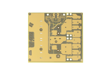
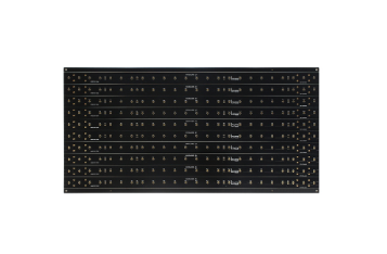
Are you eager to know how PCB fabrication is done? Perhaps you need custom printed circuit boards but you want to know how they are fabricated before deciding to get them customized for you.
If that's the case, then this article is for you. Here, we will walk you through the basic steps involved in PCB fabrication. Are you ready? Then, let's get started!

The fabrication of printed circuit boards starts with the design. Firstly, the designer lays out a plan to design the PCB. He does this by using a software known as Extended Gerber.
While designing the PCB, the software, the software encodes all the requirements for the PCB such as the number of solder masks, the number of copper layers, and other components required.
After designing the PCB with the software, the designer examines it to ensure there is no error before sending the design to the PCB fabrication department to build the PCB.
When the design reaches the PCB fabrication house, an engineer checks the design to determine if there is any flaw or error.
Furthermore, the engineer reviews the PCB design by going over every part of it to ensure all Components and structures are present and well designed.
After the PCB Design is endorsed by the engineer, it is passed to the printing stage.
The next step after the PCB Design is checked and endorsed by an engineer is to print out the design.
Unlike architectural designs, PCB designs are not printed on 8.5 × 11 sheets of paper. They are printed on a "film" by a special type of printer called a plotter printer.
The printout contains an outer layer and an inner layer which are printed in two ink colors.
For the inner layer, the circuits and copper traces of the PCB are printed in black ink, while the non-conductive layers are printed in clear ink. The reverse is the case for the outer layer.
After printing out the PCB Design on the films, holes are punched through the films. These holes are known as registration holes and they are used to properly align the films while carrying out the other processes that follow.
Following the printing of the PCB Design on a film, the building of the PCB begins.
Copper is initially bonded to the film to reveal the blueprint of the design. The copper bonded is then etched.
After this, the film panel is covered by a photo-sensitive film known as "the resist" which contains a layer of photosensitive chemicals that harden when exposed to UV light.
The resist and the film are lined up using the registration holes. Ultraviolet light is then made to pass through the translucent part of the film. This causes the resist to harden.
The hardened part of the resist indicates areas where copper and conducting circuits are built while the areas. However, the areas covered with black ink are not hardened and these indicate where the non-conductive components are built.
The board built is then washed with an alkaline solution to remove leftovers of the photo-sensitive chemicals and allowed to dry.
After this, a technician checks the built PCB to ensure there is no flaw or error.

Are you in need of a Custom PCB but you're worried about getting a reputable manufacturer for the PCB fabrication?
Don't worry, VictoryPCB got you covered. With us, you are assured of getting a fabricated PCB of high quality. Click here to get your fabricated PCB.