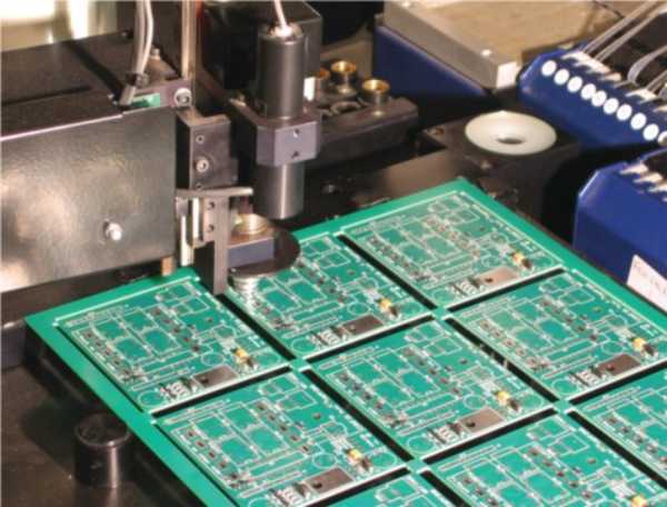
The production of printed circuit boards is a business that is profitable in absolutely any country since this component cannot be dispensed with in the creation of electronic equipment.
Craftsmen can produce such items even at home! The technology for the production of boards does not consist of stages beyond the reach of an ordinary person, and most of the components are easy to find on radio markets or specialized sites on the Internet.
Factory-designed boards are more in demand, but their production requires the appropriate equipment and adherence to clear assembly instructions.
In today's article, we will tell you more about home and factory production, as well as help you navigate the approximate cost of such a business in general.
Modern gadgets cannot imagine their existence without such a component as a printed circuit board. The workpiece is a plate of dielectric material, which contains circuits that conduct electric current.
Such "veins" can be located either on the very surface of the dielectric, or they are embedded in the inside of the base of the printed circuit board.
The purpose of the boards is to combine the components of electronic devices into a single network. They conduct electricity and connect the elements of the gadget into an integral mechanical structure. The pins at the ends of the boards are attached one to one by soldering.
• dielectric material underlying; |
• a foil pattern that acts as an electrical conductor; |
• special mounting holes; |
• pads that combine planar elements of the printed circuit board; |
• solder mask acting as a protective coating; |
• marking (in industrial production). |
If the board was manufactured on home equipment for personal use, some design components may be excluded from this list.
The classification of printing boards depends on factors such as the temperature threshold of use and the industry of application.
§ Single-sided - dielectric foil coating is applied to only one side.
§ Double Sided - Dielectric foil coating is applied to both sides of the PCB.
§ Multilayer - the dielectric base has several layers, on each of which there is a foil coating.
In the production of various electronic devices, there may be problems with the functionality of the base itself. Too brittle dielectric becomes a problem in smartphones with a flexible display, and the operation of a typical board at elevated temperatures leads to its melting and, accordingly, failure.
The increasing range of products has led to the emergence of new solutions for the implementation of components. This forced the PCB industry to introduce yet another classification based on the properties of the dielectric base material. Terms such as rigid and flexible printing boards have appeared in the technical literature.
There are also separate technological solutions that take into account the peculiarities of the use of boards for printing (high/low frequency, temperature, etc.).
The technological process of manufacturing printed circuit boards contains four main stages, each of which is divided into more local tasks that require expensive equipment and a prepared place.

Before starting production, you should worry about the preparation of materials and equipment. A list of all the necessary "raw materials" for the production of printed circuit boards is given in the table below. Classification based on the number of layers was taken into account.
The workpiece is formed from a foil dielectric material. The dielectric in industrial production is fiberglass (90% of cases) or textolite with a fabric or paper base.
The selection of the thickness of the workpiece is based on the very requirements in the order - the higher the strength and electrical conductivity, the thicker the base. In non-target production, an average thickness indicator is used - the equipment is adjusted to 13-14 millimeters.
1. Cut out the required shape on the equipment.
2. Prepare sheets of aluminum foil.
3. Apply foil to the cut piece. The thickness of the application depends on the purpose for which the board will be used.
A separate production group is made up of aluminum boards for printing - they are used in lighting equipment when for the operation of the component it is necessary to obtain conductivity through the entire surface of the board.
§ With external oxidation - a solid oxidized aluminum sheet, along the perimeter of which there is a copper foil. Other metals can be used, but their use requires the preliminary application of a thin layer of dielectric.
§ Full oxidation - the drawing by the equipment is introduced into the very basis of the material, therefore the processing falls on a large part of the depth of the workpiece. The exact value is calculated by the equipment according to the template set by the system.
In practice, the first method belongs to the more economical type of production. The entrepreneur reduces the time spent by 50-70% + does not buy additional modules for equipment.
The most time-consuming stage of production requires large investments in auxiliary raw materials and equipment.
To get a printed circuit board drawing, use one of 3 methods, or a combination of them.
1. Chemical.
It includes two stages - adding a mask to a blank with a foil layer and removing the excess by bombarding it with chemical particles. From the equipment, you will need a photoresist, a photomask, and a source of ultraviolet radiation here.

The entire surface of the workpiece is filled with photoresist (liquid or film), and then the paths of the electrical conductor are illuminated through the template with ultraviolet light.
The unprotected area is washed with a chemical solution (ferric chloride or copper sulfate), after which the foil layer is removed and only an electrically conductive pattern remains.
2. Mechanical.
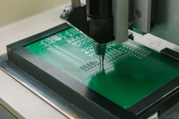
Implementation requires special equipment for mechanical action, which can remove unnecessary areas of foil on the surface of the workpiece according to the template.
3. Laser.
Previously, this method was practically not used due to the increased reflective properties of copper and aluminum. But progress does not stand still, and in 2018 laser equipment can finely tune the wavelength, which allows the installation to be used even on surfaces with high reflection parameters.
In industrial production, the most popular was and remains the method of drawing a picture using mechanical equipment. The entrepreneur does not need to worry about the mass of additional funds that are required for chemical engraving, and the use of laser equipment is too expensive.
Drawing is only the first step in the processing of a printed circuit board blank. Further, the element goes through four more intermediate technological stages until it acquires the desired form.
Holes are punched by special mechanical or laser equipment. The second option is used for finer work when it is unrealistic from a physical point of view to implement an action using mechanical processing.
1. Mechanically.
For implementation, high-precision equipment (for industrial production) and material (conductive adhesive or rivets) are required.
This method is very expensive to use, therefore it is used only selectively - for high-precision printed circuit boards, or metallization at home.
2. Chemically.
Holes are metalized by sediment accumulation on the copper billet. This process precedes the direct drawing of the pattern on the form itself.
The second method is easy to implement in industrial production, but it is rarely used for home use due to the abundance of technological nuances and duration.
It is used only for multilayer printed circuit boards that contain more than one layer.
This process precedes the plating of holes, since pressing ready-made blanks can damage the outer layer of insulation and the copper sprinklings themselves.
1. Preparation of layers that will be located in the middle and drawing of a picture. |
2. Pressing boards in a pressure oven - so-called prepregs are used as gaskets. |
3. Drilling holes. |
4. Metallization. |
5. Etching of the foil of the outer layers. |
The vias can also be formed before pressing. Then, the functionality of printed circuit boards expands, but the cost of production increases by 30-40%.
The use of "stubs" requires the entrepreneur to find a reasonable compromise between the profitability of production and the cost of the manufacturing process itself, including the cost of equipment.
§ electronic filling in automotive production;
§ stuffing of medical equipment;
§ industries related to computer technology;
§ large and small household appliances + measuring instruments.
The total cost of starting a business is at least $75,000. This includes the cost of materials, salaries of employees, equipment, rental of premises, marketing campaign, and additional costs for implementation.
The average payback for one PCB production line is at a level of 24-30 months, provided that your financial plan provides for additional expense items (repairs, maintenance of equipment, etc.).
PCB manufacturing is a highly profitable business with a long payback period. Not everyone is ready to wait more than 2 years to win back their own money. However, if the business is successful and the potential for expansion, you can cut this period in half, and further profits will grow monthly.