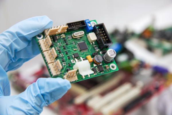
This post is the first in a series about PCB design. This part is mainly about the details you need to know and use before starting the PCB layout (from now on, the abbreviation PP will be found in the text), while the second part will be mainly about the design of the printed circuit boards themselves and post-processing.

Breadboards are good for prototyping and a very useful tool, but when you need to do something serious, you need to know how to make your PCB.
Creating a PCB is not easy, but with a little perseverance and time, this guide will help you create your first PCB.
When you work at your computer, any task seems abstract, but do not forget that you work with real physical environments and materials. Before starting to study the design of boards, it would be nice to understand how they are made.
If you know what and how it is done, you can safely proceed to the next section.
First, let's look at what materials are used for manufacturing. The base for the PCB is made of a solid non-conductive material. This material is covered with a layer of copper (or other metal), which forms the conductive layer.
Usually, the base is fibreglass, known as FR-4. This is the most commonly used material because it is fire-resistant, cheap, and has low intrinsic conductivity.
Other types of materials are used for high-performance (RF) circuits, such as ceramic or PTFE. Within the framework of these articles, we will not touch on high-frequency circuits. When you send your PCB design to manufacturing or make your board, electrical connections are usually made by removing selected sections of copper from a common conductor layer.
Single-layer PCBs are very easy to manufacture and design. The cheapest PP variant is one-sided, i.e. on fibreglass, only one layer of copper is used. If you are going to make PP at home, it will most likely be one-sided. Still, suppose your board layout does not fit in one layer. In that case, you will have to use external jumpers for electrical connections, which can already be inconvenient when mounting radio components.

Most commercial and hobby projects are built on two-layer printed circuit boards. Their use allows you to develop more complex and elegant board design solutions.
The more complex structures become, the more additional layers of metallization PP requires. Usually, two layers are enough, and if there is no need to add more layers, then it is better not to do this because multilayer boards are much more expensive to manufacture.
As mentioned above, copper tracks (electrical connections) are created by removing excess copper from the metallized layer's surface. The second article will discuss more details about the important aspects of electrical connections.
One of the main components of PCBs is vias, used in dual and multilayer boards to electrically connect one plating layer to another.
1. Through-vias - the most commonly used type, the hole is drilled through the entire board and plated to create electrical contact with the layers.
2. Blind vias - holes connecting the outer layer with one or more inner ones.
3. Hidden (buried vias) - vias that do not go outside and connect the signals on the inner layers.
4. Micro-via or uVia - micro-holes or holes of small diameter and shallow depth, made by laser or drilling with depth control and connecting the outer layer to the inner.
That's all you need to know about vias.
Let's analyze a few more concepts for building printed circuit boards and touch on some other layers of PCB, the purpose of which needs to be understood.
1. Soldermask - if you ask any person what a board is, he will say it is something green. This green one is the solder mask, which protects the PCB and prevents solder paste from getting on unwanted electrical contacts on the board. And by the way, it is not necessarily green, but almost any colour. It all depends on the board manufacturer.
2. Fiducials - This special marking on the board allows automatic component mounting systems to calibrate and correctly install elements on the board during installation. They are small circles of metal not covered by a solder mask.
3. Silkscreen - this is another layer that is applied to the board during production. Silk screen printing is drawings on the board that give hints to the user, identify the component on the board by placement or value, and other information.
4. Copper fills - sections of copper that are electrically connected to ground or power; creating polygons is a very important part of PCB design. Polygons reduce device noise and remove excess heat from powerful active components.
Before considering board design or device schematics, you must know what you want to design. You must consider what you want to build and choose the right components.
The first step to successful device design is having the right goals for what you want to achieve. You should always set smart goals for your project, which means:

1. Specific
2. Measurable
3. Achievable
4. Realistic
5. time-bound
For example, I started working on a personal project for my needs. The light in the bathroom in my apartment is dim in the evening, but when I turn on the artificial lighting, the light is quite bright and not uncomfortable.
It would be possible to buy a lamp of less power, but let's say they are not on sale or there is nowhere less. And I decided to make my lamp which will change colour and brightness and be controlled wirelessly.
Sounds pretty cool; before the idea gets out of my head, we sit at the computer and start planning. At this stage, my goals are very broad:
1. the lamp should be multicolour
2. dimmable
3. wireless control
None of these goals is specific to the project. What is meant by multicolour? Two, three or any number of colours? What is dimmable? Wireless control, how? Wifi, Zigbee, Bluetooth or maybe voice? All ways are possible.
· Continuously adjustable high-brightness RGB LEDs covered with acrylic for even light diffusion.
· Brightness control that will allow me to choose any brightness from completely off to the maximum brightness of the LEDs.
· Bluetooth Low Energy 4.0 interface to control parameters from iOS and Android devices.
Now all our goals are quite specific.
Now that you have a clear idea for your project, it's time to start designing. Before you start looking for components and drawing schematics, I suggest developing a clear picture of how your design should function. We need to draw a functional diagram of the device, what is connected with what and how it works.
You don't yet know what kind of power supply you need or what connectors should be on the board, but you already know how the components will be connected and what additional components will be needed in the project.
This is a good time to consider the aesthetic aspect of your design. Do you want to fit the board into a specific form factor? Should ergonomics be considered? Can you open your project in a year and understand how it works? These seemingly insignificant details distinguish good design from very good design.
This may be the most tedious step in the design process, but it is key to the project's success. Choosing the right components will determine whether you complete a project successfully or abandon it in desperation.
Integrated circuit manufacturers work hard to create the most functional components at the lowest cost. However, not all companies are still equal in this race, especially regarding the ease of use of components.
When choosing among the millions of different components on the market, giving a complete selection guide is very difficult. Still, I can provide a few tips to help you choose the best components for your application.
Choose components that are in abundance and available from different distributors. The last thing you want to do is put your project on hold for a few weeks or even months just because a key component of your project is out of stock with the vendor.
Sometimes components are discontinued, and you may have to change the project after a short period; however, if your device is in a single instance, this does not play a significant role.
Many online stores provide very functional filters on the site by component parameters, as well as by cost and availability. Use them, select components with optimal parameters for you, and then filter them by cost.
Many components are sold only in minimum quantities, starting from 1000 pieces.
When choosing components, pay attention to the case in which it is produced. You should not buy a component that you cannot sell later.
Before buying, be sure to study the documentation for the component so that in the future, there will be no problems with its use in the project.
After all, components are selected, you can order them. I like to order through online stores like mouser.com or digikey.com. This, of course, is purely my preference. If you know other relevant suppliers, you can write about them in the comments.
The final stage before starting to work with the software is to transfer some of the key points of the project to paper. The most suitable option is to paint each block separately on different notebook pages.
You can also make all the necessary notes about what works and what this or that pin is responsible for. Also, enter additional information that will be needed during the design process. For example, it can be tedious to look for the I2C addresses of the microcircuit in the datasheet and enter them in a notepad.
After you have completed all the notes, you can proceed to the design process of the printed circuit board itself.