Professional PCB Manufacturer

Professional PCB Manufacturer
When selecting a printed circuit board, thickness is a crucial consideration. The thickness impacts electrical properties like conductivity and resistance, which are vital to meeting your device's specifications. Functionality hinges on this aspect, as it dictates how well the PCB performs under electrical loads and mechanical stress.
Understanding the range of thickness options and aligning them with your device's requirements is key. From standard thicknesses for general use to specialized dimensions for high-power or compact devices, selecting the right PCB thickness is a balance of electrical needs and physical constraints.
This article aims to provide a comprehensive understanding of PCB thickness, factors affecting PCB thickness, and how to choose the right pcb thickness.

PCB thickness refers to the overall thickness of a printed circuit board, which includes all of its layers—such as the base material, copper layers, solder mask, and any additional layers like silkscreen. This thickness is an important aspect of PCB design because it impacts the board's mechanical strength, compatibility with components, and thermal and electrical properties.
The most widely recognized standard PCB thickness is 1.6mm (approximately 0.063 inches). This thickness is widely adopted across the electronics industry for various reasons:
Mechanical Strength and Weight: A 1.6mm thick PCB provides a good balance between being robust enough to handle during manufacturing and use, and not being excessively heavy, which is particularly important for portable electronic devices.
Compatibility with Through-Hole Components: Many through-hole components are designed with leads that fit well in a PCB of this thickness. It ensures that components can be mounted securely and that their leads are long enough to pass through the board and be soldered on the opposite side.
Ease of Manufacturing: 1.6mm PCB thickness is easier to manufacture than thicker or thinner ones. They provide enough material for secure handling and assembly without presenting difficulties in processes such as drilling, etching, and layer alignment.
Beyond the standard 1.6 mm, other common thicknesses include 0.8 mm (31 mils), 1.0 mm (39 mils), 1.6 mm (63 mils), 2.36mm (93 mils) and 3.17mm (125 mils). Here, VictoryPCB provides standard options for the overall thickness of all laminate layers on your PCB, ranging from 0.008 inches to 0.240 inches, between which you can choose depending on the application or usage area.
The standard thickness of a 2-layer PCB is 1.6mm. The total composition includes both the core material, typically FR-4, and the copper layers on each side of this core.
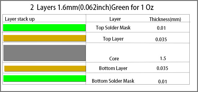
The above image outlines the specific thicknesses of the various layers that make up a standard two-layer PCB, which in total amounts to 1.6 mm (0.062 inches). Here is the detailed information presented in the image:
Top Solder Mask: 0.01 mm
Top Layer (Copper): 0.035 mm
Core (usually FR-4): 1.5 mm
Bottom Layer (Copper): 0.035 mm
Bottom Solder Mask: 0.01 mm
The most common thickness for a four-layer PCB is 1.6 mm (approximately 0.063 inches). This is the same standard thickness used for two-layer PCBs, making it a popular choice due to its balance of mechanical strength, manufacturability, and cost. It also aligns well with a broad range of component types, especially through-hole components.
Indeed, several manufacturing factors crucially impact the overall thickness of a printed circuit board. These factors must be carefully considered during the design and fabrication processes to ensure that the final product meets the specific requirements of its intended application.
The central substrate, often referred to as the core or dielectric, is the insulating layer within a PCB. It separates two conductive copper layers. The substrate is often made from materials such as FR-4 (the most common), polyimide, CEM (Composite Epoxy Material), and others, depending on the required properties like thermal stability, flexibility, and cost.
Substrate thickness in PCBs does indeed vary widely based on the application, reflecting different requirements for mechanical durability, thermal management, and spatial constraints.
For example, a thicker substrate, such as around 0.125 inches (3.2 mm), is beneficial in environments where the PCB is exposed to significant mechanical stresses. This thickness helps enhance the structural robustness of the PCB, making it more resilient to physical impacts and stresses, which are common in automotive and other heavy-duty applications.
In space-constrained applications like smartphones and wearable technology, a thinner substrate ranging from about 0.031 inches (0.8 mm) to 0.04 inches (1.0 mm) is preferred. The use of thinner substrates helps minimize the overall volume and weight of these devices, which is crucial for user comfort and device portability.
Suggested Reading: The Ultimate Guide to Insulated Metal Substrate PCBs
As a dielectric material, Prepreg provides insulation between two cores or between a core and a copper foil in a PCB. Prepreg is made from fiberglass that is soaked with a resin bonding agent and pre-cured to an intermediate stage. The term "prepreg" originates from this pre-impregnation process. Typically, the resin used is either epoxy-based or a partially cured polyimide, forming the foundational material for prepreg.
Prepreg materials are classified into three main types based on the resin content: high resin (HR), medium resin (MR), and standard resin (SR). The amount of resin combined with the fiberglass determines the thickness of the prepreg. For example, have more resin relative to the fiberglass, which can enhance their adhesive properties and electrical insulation but also increase their thickness and cost.
Prepreg thickness in PCB fabrication includes several standardized thicknesses such as pp-106 (0.002 inches), pp-1080 (0.003 inches), pp-2113 (0.004 inches), and pp-2116 (0.0047 inches). The selection depends on the desired final PCB thickness and other design specifications.
Copper layers are applied to the surface of the PCB core and within the inner layers in multilayer boards. Copper thickness is generally measured in ounces per square foot, translating into thicknesses (1 oz/ft² corresponds to about 1.4 mils or 35 microns).
Copper thickness is one of the manufacturing parameters that affects the PCB thickness. Standard copper thickness is roughly 1.4 to 2.8 mils (1 to 2 oz), but this thickness is adjusted according to the board's unique requirements. Due to material needs and processing challenges, the thicker the copper, the thicker the board and the more expensive the board will be.
Suggested Reading: Complete Guide to PCB Copper Thickness
Multi-layer PCBs consist of multiple layers of copper traces and insulating material (such as FR-4 or polyimide) stacked and bonded together. The more layers a PCB has, the thicker it will generally be. Each additional layer means adding a layer of copper and at least one layer of prepreg or core material. Common multi-layer configurations include 4, 6, 8, and up to over 30 layers for highly complex devices.
Thicker multi-layer PCBs may pose challenges in terms of manufacturability, such as difficulties in drilling and plating through holes accurately. Besides, with each additional layer, the manufacturing process becomes more complex and costly. Designers must balance the complexity of the electronic circuit with the physical space available within the device. More complex circuits typically require more layers, which can increase the PCB thickness.
The PCB thickness significantly influences three critical areas: cost, performance, and quality. Understanding how these factors are affected by PCB thickness is essential for both PCB manufacturers and their customers.
The cost of PCB manufacturing is closely tied to material usage. When fabricators produce boards that are thicker than specified, they use more material than what the cost calculation was based on, leading to losses. Conversely, if the boards are consistently thinner than specified, customers may feel shortchanged, paying more for less material. This discrepancy in material usage can be negligible for small orders but becomes financially significant for large-scale production runs.
The mechanical stability of a PCB is directly affected by its thickness. A PCB that is too thin might be susceptible to cracking under physical stress such as vibrations, which are common in many operational environments. This vulnerability can lead to severe performance degradation or even failure of the electronic device. On the other hand, a PCB that is too thick may not fit properly in compact devices, causing assembly issues and potential performance problems due to improper integration within the device structure.
During the PCB manufacturing process, boards that do not meet the specified thickness standards are likely to be flagged and rejected during quality inspections. This leads to increased scrap rates, adding to production costs. From the customer's perspective, receiving PCBs that deviate from the agreed specifications can lead to rejections during incoming quality checks. Consistently poor compliance with thickness specifications can damage a manufacturer’s reputation and lead to a loss of business.
Choosing the right PCB thickness is a critical decision that impacts the board's functionality, reliability, manufacturing process, and application. There are three types of PCBs based on PCB thicknesss: thin PCBs, thicker PCBs and extremely Thick PCB. Here's a guide on how to choose the right PCB thickness based on various application needs:
Thickness Range: 15.7 mils (0.4 mm) to 39.4 mils (1.0 mm).
Characteristics and Applications: Thin PCBs are lightweight and can be flexible, making them ideal for compact electronic devices where space is at a premium. Use thin PCBs in portable electronics like smartphones and tablets, wearable devices such as smartwatches, or in other consumer electronics where flexibility and minimal weight are crucial. These PCBs help maintain a sleek profile and reduce the overall weight of the product.
Thickness Range: 62 mils (1.6 mm) to 93 mils (2.4 mm) and sometimes even thicker.
Characteristics and Applications: Thicker PCBs offer improved mechanical strength and durability, making them suitable for more demanding environments where the board might experience physical stress or need to handle higher power densities. Opt for thicker PCBs in industrial machinery, power electronics, and robust consumer devices that require enhanced durability. These boards are better suited to withstand mechanical impacts and are preferable in applications requiring substantial thermal management.
Thickness Exceeds: 93 mils (2.4 mm), with some boards, such as backplane PCBs, being as thick as 400 mils (10.16 mm).
Characteristics and Applications: Extremely thick PCBs are typically used in critical infrastructure and specialized equipment where the PCB must support a large number of connections and high-power components. These are common in server backplanes, telecommunications equipment, and large-scale testing boards that need to be exceptionally robust and capable of managing significant thermal loads.
The substrate material's dielectric constant and the thickness of the PCB are critical because they determine the characteristic impedance of the transmission lines. The thickness of the PCB alters the distance between conductive layers, affecting capacitance and inductance per unit length, hence the impedance. Consistent impedance is essential across the PCB to minimize signal reflections and ensure accurate signal transmission. Designers need to precisely calculate and simulate to meet the impedance requirements of high-frequency components and systems.
In high-frequency circuits, signal attenuation can be a concern. Thicker PCBs can increase dielectric losses, leading to reduced signal quality. The choice of substrate material becomes significant here, as materials with lower loss tangents, such as Rogers or Teflon, are preferred over standard FR-4 for their better performance at high frequencies, despite being more expensive.
Thicker PCBs offer improved shielding against electromagnetic interference (EMI), beneficial for devices sensitive to EMI or operating in high-noise environments. However, the benefits of increased thickness for better EMI shielding need to be weighed against potential drawbacks such as higher weight and more complex manufacturing processes. Additional methods like using multiple ground layers, shielding enclosures, or specialized EMI shielding coatings might be effective alternatives.
Effective thermal management is crucial in high-frequency applications due to the higher heat generation. While thicker PCBs can help in heat dissipation, incorporating thermal vias or heat sinks might be necessary to manage the thermal load effectively.
High-frequency PCBs require precision in manufacturing to maintain tight tolerances essential for consistent impedance and minimizing signal loss. This includes precise control over etching processes to maintain accurate trace widths and spacing.
Looking for a PCB that meets your exact specifications? Look no further than VictoryPCB, a professional PCB manufacturer that combines expertise with precision to deliver high-quality circuit boards tailored to your needs. Whether it's for high-frequency applications, compact devices, or power-intensive operations, VictoryPCB has the capability to manufacture PCBs that match your required thickness, durability, and performance standards. Contact VictoryPCB today to get a quote by sales@victorypcb.com.


