Professional PCB Manufacturer

China PCB Manufacturer
You are here:

Double-sided PCB

double sided pcb

What is Double Sided PCB

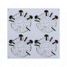
A double-sided PCB (Printed Circuit Board) is a type of PCB that has copper traces and components on both sides of the board. This allows for more complex circuitry to be created and more components to be added in a smaller space than a single-sided PCB.

Double sided pcb features two sided traces with a top and bottom layer, while single side PCB has a conductive layer on one side of PCB. Double-sided PCB has a higher density without the need for point-to-point soldering since the PCBs can be mount conductive copper and components on both sides of the circuit board.

Double sided printed circuit boards have become more and more popular in the PCB industry. Compare to single-sided PCB, and double side PCB is so complex that it can widely use higher technology electronics, vending machines, power supplies, led lighting, and many more applications.

Capabilities in Manufacturing Double Sided PCB

Victory PCB is a professional pcb manufacturer that can produce high-quality double sided PCB products. Check our PCB manufacturing capabilities in the following table:
CircuitBase Copper Thickness (OZ)1/3 OZH OZ1 OZ1.5-2 OZ3 OZ4 OZ5 OZ6 OZ
Inner LayerMinimum Trace Width   (mm)/0.100.1250.200.250.300.350.40
Minimum Trace Spacing (mm)/0.100.1250.150.250.300.350.40
Outer   LayerMinimum Trace Width   (mm)0.0750.100.1250.200.250.300.350.40
Minimum Trace Spacing (mm)0.0750.100.1250.150.250.300.350.40
Solder MaskMinimum Solder Mask Opening(single side)(mm)0.050.050.050.050.0250.000.000.00
Minimum Solder Mask Bridge (mm)0.0750.090.090.100.1250.150.1750.20

Benefits of Double Sided PCB Boards

Double-Sided PCBs have two-sided traces, which provide many benefits for various applications. Here are a few advantages of using double-sided PCBs:

  • Relatively lower costs: Double-sided PCB has a lower cost than multilayer PCBs.

  • Increased circuit density: Double-sided PCBs can be added more components that effectively increase the circuit's density. It's better to have some components connected to the bottom side rather than all on one side.

  • More flexibility and reliability: Double-sided PCB comes with both the top layer and bottom layer, so you can use the bottom layer as a ground copper pour, which provides more flexibility. The reliability is very high because the holes are chemically cleaned and activated to ensure good plating and connection between the top and bottom layers.

  • Reduced board size: Using two sides instead of one also allows for a smaller board size overall, which can be important when building small-scale, integrated devices.

  • Numerous applications: Double-sided PCBs have the circuit complexity to be used in many common electronics at a reasonable price. Use double-sided PCBs to create popular electronics for everyday use.

  • Suitable for sinking and sourcing current: You can use the bottom layer of a double-sided PCB as a ground copper pour for sinking and sourcing currents. Redirect your PCB’s current while leaving the top layer free.

Double-Sided PCB Design

Many elements of double-sided Printed Circuit Board designs are similar to single-sided PCB or multilayer PCB designs. To get started creating a double-sided PCB, you’ll need to create an electronics schematic for your board using a high-quality schematic editor. This shows designers exactly how elements in your circuits link together into a full device. You’ll need to specify ground plane and power connections directly on your board rather than incorporating power and ground planes that would appear in multilayer boards.

Getting started with your actual Printed Circuit Board requires capturing your schematic as a layout. You’ll need to start arranging your components in a way that satisfies your design rules, routing constraints, and mechanical constraints imposed by your packaging.

Applications Of Double Sided PCBs

Double-sided PCB has circuit complexity and can be used in a wide range of applications. If you use single-sided PCB or multiplayer PCB, it will fail to meet the project's requirements. Applications of double-sided PCBs include (part of applications, not all):

  • Power conversion

  • Converters

  • UPS power system

  • Automotive dashboards

  • Test Equipment

  • Control relays

  • Hard Drives

  • Power Monitoring

  • Amplifiers

  • Vending machines

  • Traffic systems

  • Car dashboards

Double Sided PCB FAQs

  • 1. What is the difference between single and double sided PCB?

    Single-sided layer boards have just one layer of base materials, known as a substrate. A double-sided PCB has more than a single layer board but fewer than a multi-layer.

  • 2. Where are double sided PCBs used?

    The following are applications in which Double Sided PCBs can be used including industrial controls, power supplies, converters, instrumentation, UPS systems and power conversion.

  • 3. How thick is a 2 layer PCB?

    2 layer PCB thickness standard thickness is 1.6mm.

  • 4. How does double-sided PCB work?

    These PCBs contain a single layer of base substrate with conductive layers on both sides. On both sides of the board, a solder mask is put. Circuits on one side of the PCB can connect to circuits on the other side to conductive holes in the board. Both sides of electronic components are soldered.

  • 5. What is the soldering process in double-sided PCB?

    Soldering two-layer boards is a time-consuming operation. However, you can use a pick and place machine to solder your board faster than soldering by hand. Moreover, you can also do using CNC Milling Machine.

  • 6. Why use double sided PCB?

    The advantages of using double-sided PCBs in your upcoming project include: More space for components: By having conductive layers on both sides, a double-sided PCB has twice the room for components as a single-sided PCB. Increase circuit density and complexity with ease.

  • 7. What is double sided PCB vs multilayer PCB?

    Multilayer PCBs are printed circuits made up of more than two layers. They must therefore have at least three layers of conductive material within the insulating material. On the other hand, double-sided PCBs only have two layers of conductive material, the top and the bottom.

  • 8. What is 2 layer and 4 layer PCB?

    2 layers PCB has two sided traces with a top and bottom layer, while 4 layers PCB has 4 layers. If you have a better understanding of two types of PCB boards, you will find that there are many differences in how they are constructed and how to work.

Get custom double sided printed circuit boards that authenticates your business products and makes it an element for quick turnaround at a first go! At VictoryPCB, we work with each customer to ensure they get the boards they need, the way they need them. Contact us today for a quote for your specifications.


×

Contact Us

×

Inquire

*Name
*Email
Company Name
Tel
*Message

By continuing to use the site you agree to our privacy policy Terms and Conditions.

Recruit global agents and distributors Join us

I agree