Choosing between PCB via in pad and dog-bone routing affects BGA fanout, routing density, signal integrity, and manufacturing cost. Both methods connect BGA pads to internal PCB layers, but differ in via placement and fabrication requirements.
The right choice depends on BGA pitch, available routing space, electrical performance, and the manufacturer’s capabilities.
Both structures provide electrical connections between BGA pads and other PCB layers. The main difference is whether the via sits directly inside the component pad or connects through a short escape trace.
Via in pad places a via directly inside a component pad, eliminating the separate escape trace between the pad and via. This arrangement saves surface routing space and provides a shorter electrical connection.
For solderable BGA pads, the via generally requires filling and copper capping to create a flat surface. This process is commonly known as via-in-pad plated over (VIPPO).
Dog-bone fanout connects a BGA pad to a nearby via through a short trace. The via sits outside the component pad, creating a pad-to-trace-to-via connection.
This approach is common in conventional BGA layouts because it usually avoids the additional filling and capping processes required by via in pad. However, the escape trace and via need sufficient space between adjacent pads.
The two fanout methods differ in routing space, electrical path, and manufacturing requirements.
| Comparison Factor | Via in Pad | Dog-Bone |
| Via location | Inside the component pad | Outside the component pad |
| Escape trace | Usually eliminated | Required |
| Routing density | Higher | Depends on available spacing |
| Electrical path | Shorter connection | Additional trace segment |
| Via filling | Usually required for solderable pads | Usually not required |
| Manufacturing complexity | Higher | Lower |
| Fabrication cost | Generally higher | Generally lower |
| Typical application | Fine-pitch BGA and dense HDI | Conventional BGA layouts |
Via in pad is not automatically the better option. Its routing and electrical benefits should justify the additional fabrication requirements and cost.
The package pitch and available routing space provide the starting point for selecting a fanout structure. Electrical requirements and total fabrication cost should also be considered.

As BGA pitch decreases, the space between adjacent pads becomes more limited. A dog-bone structure may not accommodate the required trace width, via diameter, and electrical clearance.
Via in pad allows signals to connect directly beneath component pads and escape through internal layers. This makes the method suitable for dense HDI layouts and compact packages.
For example, VictoryPCB offers a 4 Layer PCB with Via in Pad and Impedance Control, providing a product reference for this fabrication structure.
When the BGA pitch provides enough space for escape traces and vias, dog-bone routing is often the more economical option. It avoids many of the special processes associated with via filling and copper capping.
The short escape trace also provides flexibility when routing signals to different layers. For larger-pitch packages, this approach may support the required fanout without increasing the PCB layer count.
Via in pad removes the short trace between the BGA pad and via, potentially reducing connection length and associated parasitic effects. This can benefit high-speed layouts where via transitions and routing geometry affect signal integrity.
However, via placement alone does not determine electrical performance. Reference planes, return paths, via stubs, impedance control, and stackup design remain important.
Via-in-pad structures require additional process controls because the via is located within a solderable component pad.
An open via inside a BGA pad can draw molten solder into the hole during reflow. This may reduce the solder available for the joint and contribute to weak connections or voiding.
For solderable pads, the manufacturer generally fills the via and applies copper plating over the opening. The resulting surface should be sufficiently flat for solder paste printing and component placement.
Uneven filling or copper capping can create depressions or raised areas on the pad. These irregularities may affect solder paste deposition and component seating.
Specify the filling material, capping requirements, and acceptable surface condition in the fabrication documentation. Microsection inspection and surface checks can help verify process quality.
For additional design considerations, refer to VictoryPCB’s guide to PCB microvia design and filling.
A manufacturable BGA layout requires clear design data and early coordination with the PCB manufacturer.
Review the BGA pitch, pad diameter, ball arrangement, and escape direction. Compare these dimensions with the proposed trace width, via diameter, and clearance rules to determine whether dog-bone routing is feasible.
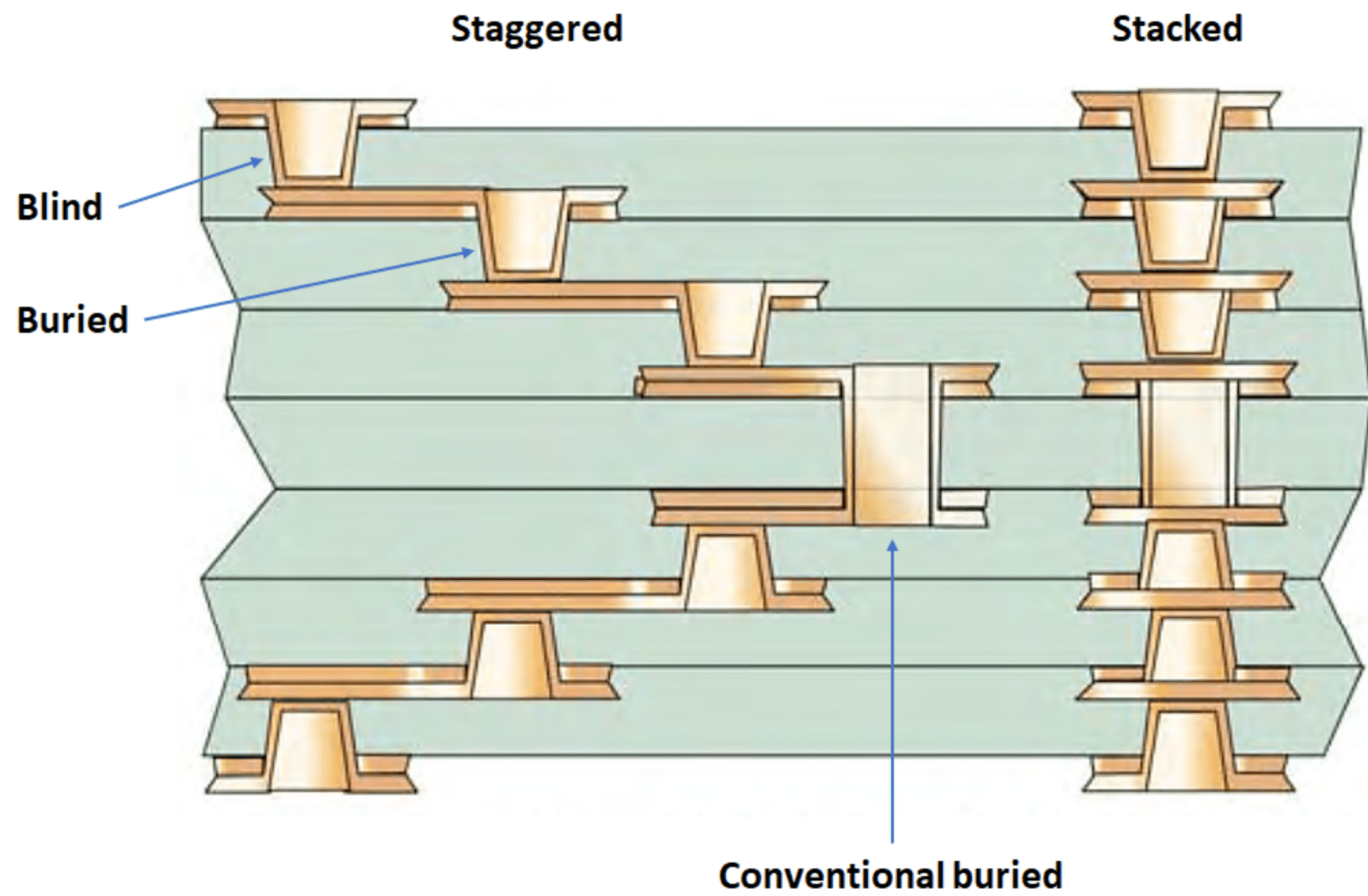
If conventional fanout cannot meet the spacing requirements, consider via in pad or an HDI stackup. A 14 Layer High Density HDI PCB is an example of a multilayer structure intended for high-density circuit applications.
Before finalizing the layout, confirm the manufacturer’s supported via dimensions, microvia structures, filling methods, copper capping process, and inspection capabilities.
Also compare the total cost of each option. Via in pad may require additional processing but reduce routing layers, while dog-bone may have lower process costs but need more routing space or additional layers.
Provide the manufacturer with the BGA footprint, stackup, drill data, copper requirements, and assembly specifications for a design-for-manufacturing review.

No. Via in pad is useful for fine-pitch and high-density layouts, but requires additional fabrication processes. Dog-bone routing is often more economical when sufficient routing space is available.
For solderable BGA pads, via filling and copper capping are generally recommended to prevent solder loss into the via and create a flat pad surface. The exact process depends on the via structure and assembly requirements.
It can shorten the connection between a BGA pad and an internal layer, potentially reducing parasitic effects. However, signal integrity also depends on the PCB stackup, return paths, via stubs, and routing geometry.
PCB via in pad supports dense BGA routing, while dog-bone fanout offers a simpler and generally lower-cost alternative when sufficient space is available. Contact VictoryPCB to review your BGA layout and manufacturing requirements.