PCB impedance control is essential for high-speed and high-frequency circuits. Incorrect trace geometry, dielectric properties, or layer spacing can cause signal reflections and transmission errors.
Understanding design and manufacturing factors helps engineers maintain signal integrity.
PCB impedance control means maintaining a specified characteristic impedance along signal paths. It is used in high-speed digital circuits, RF systems, and differential signaling.
Characteristic impedance describes the relationship between voltage and current as a signal travels along a transmission line. It depends on trace geometry, dielectric properties, and the reference plane.
Common targets include 50 ohms for many single-ended RF signals and 90 or 100 ohms for certain differential interfaces. Follow component datasheets and system specifications when selecting the target.
Not every trace needs controlled impedance. Identify critical paths based on interface requirements, signal rise time, and operating frequency.
Common examples include USB and Ethernet differential pairs, PCIe connections, high-speed serial interfaces, and RF transmission lines.
PCB impedance depends on several interacting parameters. Changing one dimension can affect the final value.
A wider trace generally has lower impedance when other parameters remain constant. For differential pairs, trace width and conductor spacing determine differential impedance. Copper thickness and etching also affect finished dimensions.
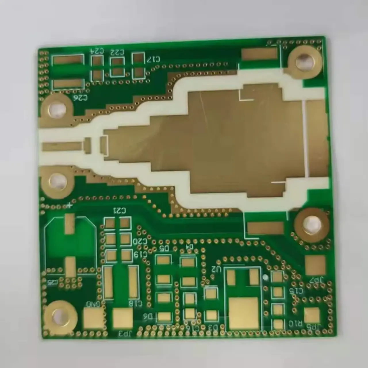
The dielectric constant (Dk) affects signal propagation and impedance. Material selection should consider frequency, signal loss, thermal requirements, and availability.
High-frequency designs may require specialized laminates rather than standard FR-4. A 2L Rogers 4350B PCB is one example of a board using Rogers material.
The distance between a signal trace and its reference plane affects impedance. Provide continuous reference planes beneath critical signals. A PCB stackup calculator can help evaluate layer arrangements and estimate impedance.
Trace geometry, reference planes, and routing conditions must work together.
Two common structures are microstrip and stripline.
| Structure | Location | Main Design Consideration |
| Microstrip | Outer layer above a reference plane | Affected by the environment and solder mask |
| Stripline | Internal layer between reference planes | More controlled electromagnetic environment |
Microstrip suits outer-layer routing, while stripline provides greater shielding. The choice depends on signal and stackup requirements.
Plane splits, gaps, or large cutouts can force return current to take a longer route, increasing loop inductance and creating signal integrity problems. Avoid routing critical traces across plane gaps. When signals change reference layers through vias, provide a suitable return path.
Impedance calculators and field solvers estimate trace width, spacing, and dielectric requirements. Verify results with the manufacturer’s materials and capabilities. See these high-speed PCB design guidelines for additional routing considerations.
Manufacturing variation can cause impedance deviations even when the original design is correct.
Dielectric thickness, Dk, copper thickness, and surface roughness affect transmission line geometry and electrical performance. Confirm laminate, copper weight, and prepreg thickness before approving the stackup. Assess any material substitution for its impedance impact.
Etching determines finished trace width and sidewall profile. Over-etching narrows conductors, while under-etching leaves them wider than intended. Imaging, etching control, and trace inspection help maintain the required geometry.
Specify impedance tolerance in the fabrication documents. Provide the target value, signal layer, trace width, differential spacing, and reference plane information. Agree on tolerance with the manufacturer before production.
Design calculations establish the target; electrical testing checks the manufactured board.
Manufacturers commonly place impedance coupons in production panels. These reproduce representative trace structures for electrical measurement. Time Domain Reflectometry (TDR) measures impedance by analyzing signal reflections and helps identify deviations from the target.
Compare impedance reports with fabrication requirements. If results fall outside tolerance, the manufacturer may need to adjust trace geometry, dielectric thickness, or process parameters. First-article testing is useful for new stackups and high-speed designs.

Manufacturers need suitable materials, stackup engineering, fine-line processing, and impedance testing.
Review supported layer counts, material options, minimum trace width and spacing, copper thickness, and testing methods. The Green 4 Layer PCB with Via In Pad & Impedance Control is an example combining multilayer construction and impedance control.
The 10 Layer Immersion Gold PCB is another multilayer example. Confirm actual impedance capability for the specific stackup and design.
Provide target impedance, signal layers and reference planes, trace width and differential spacing, stackup and dielectric requirements, acceptable tolerance, and test coupon or reporting requirements. Early review helps identify conflicts.

50 ohms is common for single-ended RF and high-speed signal paths. Differential interfaces may use 90 or 100 ohms, depending on the protocol.
Yes. Board thickness affects impedance through dielectric spacing between signal traces and reference planes. The result also depends on stackup and trace geometry.
Manufacturers commonly use TDR testing on impedance coupons to measure representative transmission lines and compare results with the specified tolerance.
PCB impedance control depends on coordinated design and manufacturing. Proper stackup planning, trace geometry, material selection, process control, and TDR verification help maintain signal integrity.
Contact VictoryPCB to review your impedance requirements and discuss manufacturing feasibility.