PCB aspect ratio affects drilling feasibility and hole plating reliability. As board thickness increases or drill diameter decreases, achieving uniform copper plating inside through holes becomes more challenging.
Understanding this relationship helps engineers select suitable drill sizes, reduce plating defects, and improve PCB manufacturing reliability.
PCB aspect ratio describes the relationship between a hole’s depth and its diameter. It indicates how deep and narrow a hole is, affecting drilling difficulty and copper plating uniformity.
For a plated through hole, the aspect ratio is calculated by dividing the PCB thickness by the drill diameter:
Aspect Ratio = Board Thickness / Drill Diameter
For example, a 2.0 mm thick PCB with a 0.2 mm drill diameter has an aspect ratio of 10:1. A higher ratio indicates a deeper, narrower hole that is more difficult to plate uniformly.
Two product examples illustrate how these dimensions apply to multilayer PCB designs.
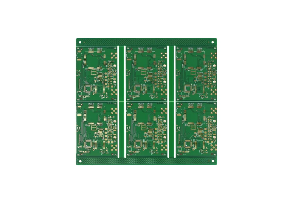
The 14L High Density HDI Immersion Gold PCB and High Quality Professional Customized ENIG Aircraft PCB both feature a 2.0 mm board thickness and a 0.2 mm minimum hole size. These specifications provide practical references for evaluating drill dimensions in multilayer designs.

Different via structures have different depths, which affect their aspect ratios.
| Via Type | Hole Depth | Design Consideration |
| Through hole | Entire board thickness | Requires plating across all layers |
| Blind via | Surface to an internal layer | Depends on the connected layer depth |
| Buried via | Between internal layers | Depends on the distance between connected layers |
Engineers should also distinguish between the initial drill diameter and the finished hole diameter because copper plating reduces the final opening.
Drill diameter determines how easily plating chemicals reach the inside of a hole. When a hole is narrow relative to the board thickness, solution circulation and current distribution become more difficult to control. This can result in uneven copper deposition, particularly in deeper sections.
As the aspect ratio increases, plating solution exchange inside the hole becomes more difficult. Maintaining consistent chemical conditions and copper deposition throughout the hole requires tighter process control.
Smaller drill diameters also increase drilling challenges. Drill bit wear, hole wall quality, and debris removal can affect the subsequent plating process.
Insufficient plating control can lead to several defects:
These defects can weaken electrical connections and reduce long-term reliability. Therefore, aspect ratio should be considered during PCB design rather than treated only as a manufacturing issue.
The practical aspect ratio limit depends on the manufacturer’s drilling and plating capabilities. A design that works with one production process may require adjustments when transferred to another facility.
Mechanical drilling is commonly used for conventional through holes, while laser drilling is typically used for smaller microvias in high-density interconnect designs. The choice depends on drill diameter, board thickness, via structure, and manufacturing requirements.
Understanding the PCB drilling process helps engineers assess whether the manufacturer’s drilling capabilities meet the required aspect ratio.
Drilling capability alone does not determine the achievable aspect ratio. Plating equipment, solution circulation, current density, and process parameters also influence copper distribution inside holes.
Manufacturers must control these conditions to maintain sufficient copper thickness throughout the hole barrel. Engineers should therefore evaluate both drilling and plating capabilities when reviewing manufacturing limits.
Optimizing drill dimensions and via structures can improve production feasibility. Engineers need to balance electrical performance, mechanical requirements, available board space, and manufacturing capabilities.
Select drill diameters based on component mounting, electrical connections, and routing requirements. Where space allows, a larger drill diameter can lower the aspect ratio and improve plating uniformity.
Via structures also affect the aspect ratio. Through holes span the entire board, while blind and buried vias connect selected layers. Their different depths result in different aspect ratios.
Before releasing production files, engineers should:
These checks help reduce unnecessary design changes and manufacturing risks.
Optimizing the aspect ratio improves manufacturing feasibility, but it does not automatically guarantee reliable plated holes. Inspection and testing are necessary to confirm copper distribution, hole wall condition, and electrical performance.
Microsection analysis is commonly used to examine the internal structure of plated through holes. A prepared PCB cross section allows inspectors to measure copper thickness and identify defects such as voids, cracks, or uneven plating.
This method provides direct evidence of plating quality and helps determine whether the hole structure meets the specified manufacturing requirements. The PCB microsection analysis process provides further details on this inspection method.
Other testing methods provide additional quality information:
Combining physical inspection, thermal evaluation, and electrical testing provides a more complete assessment of plated hole quality.
After establishing design and quality requirements, engineers should compare them with the manufacturer’s actual production specifications. This helps confirm whether the selected drill dimensions and board thickness are suitable for the available processes.
Review the manufacturer’s layer count, minimum drill diameter, board thickness, and plating capabilities before finalizing the design.
Established in 2005, VictoryPCB supports 1–16 layer boards, with a minimum hole size of 0.1 mm. Its facilities cover approximately 30,000 m², with a monthly production capacity of 60,000 m².
Actual manufacturability depends on board thickness, drill diameter, via structure, and plating conditions. Engineers should confirm these details with the manufacturer before production.
Provide the manufacturer with the PCB stackup, board thickness, drill file, finished hole dimensions, copper requirements, and relevant quality standards.
Early engineering review helps identify aspect ratio risks and determine whether drill dimensions or via structures need adjustment, particularly for thick boards and small holes.

Yes. PCB aspect ratio can affect signal performance via geometry and interconnection characteristics. Signal integrity also depends on via length, impedance control, pad dimensions, and PCB stackup.
Drill diameter, board thickness, plating requirements, and inspection standards all affect PCB fabrication costs. These factors should be considered during the design stage to balance manufacturing requirements and budget.
Define hole dimensions, copper thickness, and inspection requirements clearly during the design stage. Confirm manufacturing capabilities and conduct prototype testing before mass production.
PCB aspect ratio influences drilling feasibility and plated hole reliability. Balancing board thickness, drill diameter, and plating requirements helps reduce manufacturing risks.
Contact VictoryPCB to review your PCB design and discuss manufacturing feasibility.