A double sided flexible PCB allows electrical connections to fit into assemblies where conventional rigid boards cannot accommodate movement or limited installation space. In dynamic applications, however, repeated movement can gradually weaken conductors and material interfaces.
For engineers developing a flex circuit for repeated bending, the key challenge is maintaining electrical continuity while controlling mechanical stress throughout the service life. This requires the electrical layout, mechanical construction, and manufacturing process to be considered together.

When a flexible circuit bends, the outer side of the bend experiences tensile strain while the inner side experiences compression. Copper conductors farther from the neutral axis generally experience greater mechanical strain.
During repeated movement, this cyclic strain can cause fatigue damage. Small defects, abrupt geometry changes, and rigid features can become local stress concentration points and eventually contribute to conductor failure.
The neutral axis is the region where bending strain approaches zero. Its actual position depends on the complete stackup, including copper, dielectric layers, coverlay, adhesive layers, and stiffeners.
In a double sided structure, the position and thickness of copper on both sides affect the overall mechanical behavior. A stackup should therefore be evaluated as a complete structure rather than judging each copper layer separately.
Common failure locations include active bend zones, rigid to flex transitions, sharp trace transitions, and areas containing plated features.
Vias and plated through holes introduce relatively rigid structures into the flexible circuit. Keeping them outside active dynamic bend areas can reduce localized mechanical stress and simplify reliability validation.
Copper type affects resistance to repeated bending. Rolled annealed copper is commonly used for demanding flex applications because its structure provides better resistance to repeated flexing than conventional electrodeposited copper.
The final copper selection should also consider copper thickness, bend radius, trace geometry, and the required number of flex cycles.
Polyimide is widely used as the base material for flexible circuits because it provides the flexibility and thermal stability needed for compact bending structures. In a double sided flexible PCB, the polyimide layers work with the copper layers and coverlay to form the complete flex stackup.
For projects that require a defined layer count, thickness, copper weight, and via structure, engineers should evaluate the complete construction rather than selecting the base material alone. The available flexible PCB products can be reviewed alongside the required bending conditions and electrical requirements.
Copper thickness affects both electrical capacity and mechanical flexibility. Thicker copper generally increases the stiffness of a flex section, so the required current capacity and mechanical movement should be considered together.
Coverlay protects exposed conductors while preserving the flexibility required by the circuit. Its thickness and termination should be reviewed together with the copper layout and bend area.
| Material Factor | Common Flex Consideration | Effect on Dynamic Bending |
| Copper Type | RA or ED copper | Copper construction affects fatigue resistance |
| Copper Thickness | Thin to heavy copper | Thicker copper generally increases stiffness |
| Dielectric | Polyimide | Total thickness affects bending strain |
| Protective Layer | Polyimide coverlay | Protects conductors while maintaining flexibility |
| Stackup | Symmetrical or asymmetrical | Layer position affects mechanical behavior |
Directly aligning top and bottom traces over the same area can increase local stiffness in a double sided flex section.
Where the circuit architecture permits, staggering conductors between the two copper layers can distribute the copper more evenly through the flex structure. This approach can reduce localized stiffness in areas exposed to repeated movement.
Sharp corners can create localized stress concentrations in a flexible circuit. Smooth curved routing is generally preferable when traces enter or pass through a bending region.
Trace direction should be determined by the actual bending axis and movement of the assembly. Plated holes can also create relatively rigid points in a flexible circuit, so transition vias should generally be positioned in rigid or supported areas rather than inside active bend regions.
If a via must be located close to a bend boundary, its position should be reviewed against the specific stackup and expected mechanical movement.
Stiffeners provide localized mechanical reinforcement for areas such as connectors and component mounting locations. They should support these areas without unnecessarily extending into the active flex section.
VictoryPCB lists polyimide, FR4, aluminum, and steel as stiffener materials. Its published PI stiffener thicknesses include 0.05 mm, 0.075 mm, 0.1 mm, 0.125 mm, 0.15 mm, 0.2 mm, and 0.25 mm.
The manufacturer’s PCB stiffener guide provides additional information about stiffener materials, thicknesses, applications, and attachment methods.
Copper cracking can result from excessive bending strain, unsuitable copper construction, abrupt trace geometry, or excessive local stiffness.
Failure analysis should distinguish between material problems, layout issues, and manufacturing process factors. Initial electrical testing alone may not reveal fatigue that develops after repeated mechanical cycling.
Rigid to flex transitions can experience higher stress because mechanical stiffness changes between supported and flexible sections.
Coverlay termination, stiffener edges, conductor routing, and nearby plated features should therefore be reviewed as one transition area rather than as independent design details.
Connector areas often require additional mechanical support because insertion and removal forces can be transferred into the flexible circuit.
A local stiffener can reinforce the connector region while allowing the remaining flex section to move as designed. The material and thickness should match the connector structure and assembly requirements.
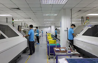
The fabrication package should clearly define copper type and thickness, dielectric materials, coverlay, stiffeners, surface finish, and expected mechanical movement.
These details allow the manufacturer to evaluate whether the proposed construction is compatible with the required production process.
General PCB manufacturing limits should not automatically be treated as limits for every flexible circuit. The actual material stackup, drilling method, thickness, and flex construction must be considered.
VictoryPCB’s manufacturing capability page lists 0.075 mm minimum trace width and spacing, while its broader manufacturing capability covers materials including polyimide and multiple surface finishes.
For this reason, critical dimensions should be reviewed against the specific flexible PCB construction before tooling.
A PCB manufacturing capability review can help identify potential conflicts between layout requirements and available fabrication processes.
Cost depends on layer count, copper thickness, dielectric construction, coverlay, stiffeners, drilling requirements, surface finish, board dimensions, and production volume.
More complex mechanical requirements can also increase engineering and manufacturing requirements. A complete fabrication specification allows the manufacturer to evaluate the actual construction accurately.
Thinner copper is generally easier to flex because it contributes less mechanical stiffness. However, current carrying requirements may require a thicker conductor.
The final copper thickness should therefore balance electrical requirements with bend radius, flex cycles, trace geometry, and total stackup thickness.
Vias are generally avoided in active dynamic bend zones because their plated structures can create mechanical stress concentrations.
Where possible, transition vias should be located in rigid or supported areas. If a via must be placed close to a bend, the design should be reviewed against the actual construction and mechanical movement.
Surface finish should be selected according to the electrical, soldering, contact, and mechanical requirements of the finished circuit.
The finish should also be considered together with the location of the flex zone and the expected mechanical movement rather than selected independently.
Reliable double sided flexible PCB design depends on matching the stackup, materials, routing, bend conditions, and manufacturing process to the required mechanical movement.
Reviewing these factors during DFM can reduce conductor fatigue, transition damage, and manufacturing problems before production.
For a design review or fabrication inquiry, contact the manufacturer through the VictoryPCB contact page.